This week ASML is making two very important announcements related to their progress with high numerical aperature extreme ultraviolet lithography (High-NA EUV). First up, the company's High-NA EUV prototype system at its fab in Veldhoven, the Netherlands, has printed the first 10nm patterns, which is a major milestone for ASML and their next-gen tools. Second, the company has also revealed that it's second High-NA EUV system is now out the door as well, and has been shipped to an unnamed customer.
"Our High-NA EUV system in Veldhoven printed the first-ever 10 nanometer dense lines," a statement by ASML reads. "Imaging was done after optics, sensors and stages completed coarse calibration. Next up: bringing the system to full performance. And achieving the same results in the field."
Our High NA EUV system in Veldhoven printed the first-ever 10 nanometer dense lines. ✨ Imaging was done after optics, sensors and stages completed coarse calibration.
— ASML (@ASMLcompany) April 17, 2024
Next up: bringing the system to full performance. And achieving the same results in the field. ⚙️ pic.twitter.com/zcA5V0ScUf
Alongside the system shipped to Intel at the end of 2023, ASML has retained their own Twinscan EXE:5000 scanner at their Veldhoven, Netherlands, facility, which is what the company is using for further research and development into High-NA EUV. Using that machine, the company has been able to print dense lines spaced 10 nanometers apart, which is a major milestone in photolithography development. Previously, only small-scale, experimental lab machines have been able to achieve this kind of a resolution. Eventually, High-NA EUV tools will achieve a resolution of 8 nm, which will be instrumental to build logic chips on technologies beyond 3 nm.
Intel's Twinscan EXE:5000 scanner at its D1X fab near Hillsboro, Oregon is also close behind, and its assembly is said to be nearing completion. That machine will be primarily used for Intel's own High-NA EUV R&D, with Intel slated to use its successor — the commercial-grade Twinscan EXE:5200 — to produce its chips on its Intel 14A (1.4 nm-class) in mass quantities in 2026 – 2027.
But Intel will not be the only chipmaker that gets to experiment with a High-NA EUV scanner for very long. As revealed by ASML, the company recently started shipping another Twinscan EXE:5000 machine to yet another customer. The fab tool maker is not disclosing the client, but previously it has said that all of leading logic and memory producers are in the process of procuring High-NA tools for R&D purposes, so the list of 'suspects' is pretty short.
"Regarding High-NA, or 0.55 NA EUV, we shipped our first system to a customer and this system is currently under installation," said Christophe Fouquet, chief business officer of ASML, at the company's earnings conference call with analysts and investors. "We started to ship the second system this month and its installation is also about to start."
While Intel plans to adopt High-NA EUV tools ahead of the industry, other chipmakers seem to a bit more cautious and plan to rely on risky yet already known Low-NA EUV double patterning method for production a 3 nm and 2 nm. Still, regardless of the exact timing for a transition, all of the major fabs will be relying on High-NA EUV tools in due time. So all parties have an interest in how ASML's R&D turns out.
"The customer interest for our [High-NA] system lab is high as this system will help both our Logic and Memory customers prepare for High-NA insertion into their roadmaps," said Fouquet. "Relative to 0.33 NA, the 0.55 NA system provides finer resolution enabling an almost 3x increase in transistor density, at a similar productivity, in support of sub-2nm Logic and sub-10nm DRAM nodes."
While neuromorphic computing remains under research for the time being, efforts into the field have continued to grow over the years, as have the capabilities of the specialty chips that have been developed for this research. Following those lines, this morning Intel and Sandia National Laboratories are celebrating the deployment of the Hala Point neuromorphic system, which the two believe is the highest capacity system in the world. With 1.15 billion neurons overall, Hala Point is the largest deployment yet for Intel’s Loihi 2 neuromorphic chip, which was first announced at the tail-end of 2021.
The Hala Point system incorporates 1152 Loihi 2 processors, each of which is capable of simulating a million neurons. As noted back at the time of Loihi 2’s launch, these chips are actually rather small – just 31 mm2 per chip with 2.3 billion transistors each, as they’re built on the Intel 4 process (one of the only other Intel chips to do so, besides Meteor Lake). As a result, the complete system is similarly petite, taking up just 6 rack units of space (or as Sandia likes to compare it to, about the size of a microwave), with a power consumption of 2.6 kW. Now that it’s online, Hala Point has dethroned the SpiNNaker system as the largest disclosed neuromorphic system, offering admittedly just a slightly larger number of neurons at less than 3% of the power consumption of the 100 kW British system.
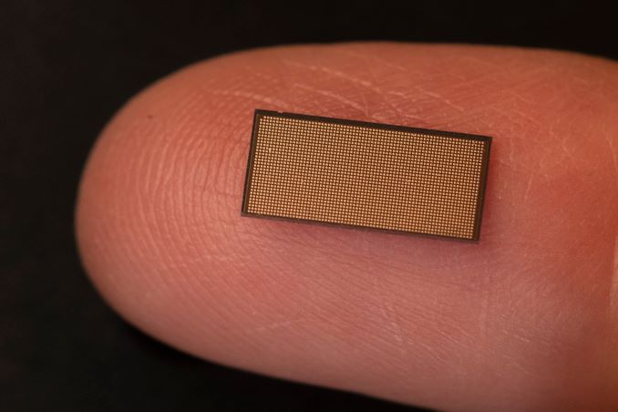
A Single Loihi 2 Chip (31 mm2)
Hala Point will be replacing an older Intel neuromorphic system at Sandia, Pohoiki Springs, which is based on Intel’s first-generation Loihi chips. By comparison, Hala Point offers ten-times as many neurons, and upwards of 12x the performance overall,
Both neuromorphic systems have been procured by Sandia in order to advance the national lab’s research into neuromorphic computing, a computing paradigm that behaves like a brain. The central thought (if you’ll excuse the pun) is that by mimicking the wetware writing this article, neuromorphic chips can be used to solve problems that conventional processors cannot solve today, and that they can do so more efficiently as well.
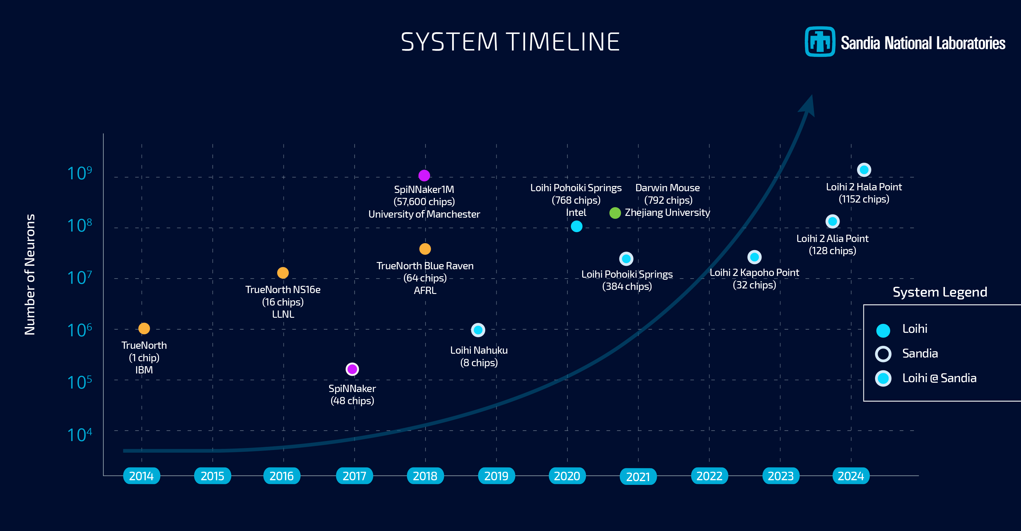
Sandia, for its part, has said that it will be using the system to look at large-scale neuromorphic computing, with work operating on a scale well beyond Pohoiki Springs. With Hala Point offering a simulated neuron count very roughly on the level of complexity of an owl brain, the lab believes that a larger-scale system will finally enable them to properly exploit the properties of neuromorphic computing to solve real problems in fields such as device physics, computer architecture, computer science and informatics, moving well beyond the simple demonstrations initially achieved at a smaller scale.
One new focus from the lab, which in turn has caught Intel’s attention, is the applicability of neuromorphic computing towards AI inference. Because the neural networks themselves behind the current wave of AI systems are attempting to emulate the human brain, in a sense, there is an obvious degree of synergy with the brain-mimicking neuromorphic chips, even if the algorithms differ in some key respects. Still, with energy efficiency being one of the major benefits of neuromorphic computing, it’s pushed Intel to look into the matter further – and even build a second, Hala Point-sized system of their own.
According to Intel, in their research on Hala Point, the system has reached efficiencies as high as 15 TOPS-per-Watt at 8-bit precision, albeit while using 10:1 sparsity, making it more than competitive with current-generation commercial chips. As an added bonus to that efficiency, the neuromorphic systems don’t require extensive data processing and batching in advance, which is normally necessary to make efficient use of the high density ALU arrays in GPUs and GPU-like processors.
Perhaps the most interesting use case of all, however, is the potential for being able to use neuromorphic computing to enable augmenting neural networks with additional data on the fly. The idea behind this being to avoid re-training, as current LLMs require, which is extremely costly due to the extensive computing resources required. In essence, this is taking another page from how brains operate, allowing for continuous learning and dataset augmentation.
But for the moment, at least, this remains a subject of academic study. Eventually, Intel and Sandia want systems like Hala Point to lead to the development of commercial systems – and presumably, at even larger scales. But to get there, researchers at Sandia and elsewhere will first need to use the current crop of systems to better refine their algorithms, as well as better figure out how to map larger workloads to this style of computing in order to prove their utility at larger scales.
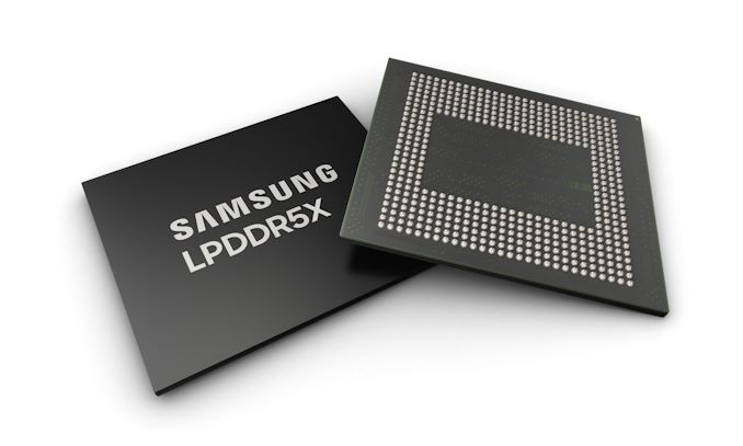
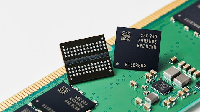
Samsung today has announced that they have developed an even faster generation of LPDDR5X memory that is set to top out at LPDDR5X-10700 speeds. The updated memory is slated to offer 25% better performance and 30% greater capacity compared to existing mobile DRAM devices from the company. The new chips also appear to be tangibly faster than Micron's LPDDR5X memory and SK hynix's LPDDR5T chips.
Samsung's forthcoming LPDDR5X devices feature a data transfer rate of 10.7 GT/s as well as maximum capacity per stack of 32 GB. This allows Samsung's clients to equip their latest smartphones or laptops with 32 GB of low-power memory using just one DRAM package, which greatly simplifies their designs. Samsung says that 32 GB of memory will be particularly beneficial for on-device AI applications.
Samsung is using its latest-generation 12nm-class DRAM process technology to make its LPDDR5X-10700 devices, which allows the company to achieve the smallest LPDDR device size in the industry, the memory maker said.
In terms of power efficiency, Samsung claims that they have integrated multiple new power-saving features into the new LPDDR5X devices. These include an optimized power variation system that adjusts energy consumption based on workload, and expanded intervals for low-power mode that extend the periods of energy saving. These innovations collectively enhance power efficiency by 25% compared to earlier versions, benefiting mobile platforms by extending battery life, the company said.
“As demand for low-power, high-performance memory increases, LPDDR DRAM is expected to expand its applications from mainly mobile to other areas that traditionally require higher performance and reliability such as PCs, accelerators, servers and automobiles,” said YongCheol Bae, Executive Vice President of Memory Product Planning of the Memory Business at Samsung Electronics. “Samsung will continue to innovate and deliver optimized products for the upcoming on-device AI era through close collaboration with customers.”
Samsung plans to initiate mass production of the 10.7 GT/s LPDDR5X DRAM in the second half of this year. This follows a series of compatibility tests with mobile application processors and device manufacturers to ensure seamless integration into future products.
Iceberg Thermal Inc. is one of the newer players in the PC cooling market. The company was founded in 2019 by an experienced team of designers and engineers setting off on their own, aiming to deliver a wide range of PC cooling products to industrial and commercial users alike. They only have a handful of retails products currently available, with the vast majority of them being CPU air coolers, but they have just launched their first liquid cooler products, the IceFLOE Oasis series.
In today’s review, we are having a look at the IceFLOE Oasis 360mm AIO (All-In-One) CPU cooler, the larger of the company's two recently-released liquid coolers. The IceFLOE Oasis CPU cooler targets the high-performance PC cooling market with a sub-$100 price point, aiming to deliver the performance needed to effectively cool a power-hungry processor without being a drain on the wallet in the process. This cooler features a 360mm radiator for an ample heat dissipation area, as well as housing for three high-airflow 120 mm fans. The IceFLOE Oasis supports a wide range of Intel and AMD socket types, making it compatible with a broad spectrum of CPUs. Additionally, it offers advanced RGB lighting, allowing users to customize the aesthetic of their cooling system.
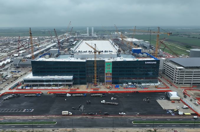
Samsung Electronics this week was awarded up to $6.4 billion from the U.S. government under the CHIPS and Science Act to build its new fab complex in Taylor, Texas. This is the third major award under the act in the last month, with all three leading-edge fabs – Intel, TSMC, and now Samsung – receiving multi-billion dollar funding packages under the domestic chip production program. Overall, the final price tag on Samsung's new fab complex is expected to reach $40 billion by the time it's completed later this decade.
Samsung's CHIPS Act funding was announced during a celebratory event attended by U.S. Secretary of Commerce Gina Raimondo and Samsung Semiconductor chief executive Kye Hyun Kyung. During the event, Kyung outlined the strategic goals of the expansion, emphasizing that the additional funding will not only increase production capacity but also strengthen the entire local semiconductor ecosystem. Samsung plans to equip its fab near Taylor, Texas, with the latest wafer fab tools to produce advanced chips. The Financial Times reports that Samsung aims to produce semiconductors on its 2nm-class process technology starting 2026, though for now this is unofficial information.
"I am pleased to announce a preliminary agreement between Samsung and the Department of Commerce to bring Samsung's advanced semiconductor manufacturing and research and development to Texas," said Joe Biden, the U.S. president, in a statement. "This announcement will unleash over $40 billion in investment from Samsung, and cement central Texas's role as a state-of-the-art semiconductor ecosystem, creating at least 21,500 jobs and leveraging up to $40 million in CHIPS funding to train and develop the local workforce. These facilities will support the production of some of the most powerful chips in the world, which are essential to advanced technologies like artificial intelligence and will bolster U.S. national security."
Samsung has been a significant contributor to the Texas economy for decades, starting chip manufacturing in the U.S. in 1996. With previous investments totaling $18 billion in its Austin operations, Samsung's expansion into Taylor with an additional investment of at least $17 billion underscores its role as one of the largest foreign direct investors in U.S. history. The total expected investment in the new fab surpasses $40 billion, making it one of the largest for a greenfield project in the nation and transforming Taylor into a major hub for semiconductor manufacturing.
The CEO highlighted the substantial economic impact of Samsung's operations, noting a nearly double increase in regional economic output from $13.6 billion to $26.8 billion between 2022 and 2023. The ongoing expansion is projected to further stimulate economic growth, create thousands of jobs, and enhance the community's overall development.
“We are not just expanding production facilities; we’re strengthening the local semiconductor ecosystem and positioning the U.S. as a global semiconductor manufacturing destination.” said Kyung. “To meet the expected surge in demand from U.S. customers, for future products like AI chips, our fabs will be equipped for cutting-edge process technologies and help bring security to the U.S. semiconductor supply chain.”
Samsung is also committed to environmental sustainability and workforce development. The company plans to operate using 100% clean energy and incorporate advanced water management technologies. Additionally, it is investing in education and training programs to develop a new generation of semiconductor professionals. These initiatives include partnerships with educational institutions and programs tailored for military veterans.
In his remarks, Kyung expressed gratitude to President Biden, Secretary Raimondo, and other governmental and community supporters for their ongoing support. This collaborative effort between Samsung and various levels of government, as well as the local community, is pivotal in advancing America's semiconductor industry and ensuring its global competitiveness.
"Today’s announcement will help Samsung bring more semiconductor production, innovation, and jobs to U.S. shores, reinforcing America’s economy, competitiveness, and critical chip supply chains," a statememt by the Semiconductor Industry Associate reads. "We applaud Samsung for investing boldly in U.S.-based manufacturing and salute the U.S. Commerce Department for making significant headway in implementing the CHIPS Act’s manufacturing incentives and R&D programs. We look forward to continuing to work with leaders in government and industry to ensure the CHIPS Act remains on track to help reinvigorate U.S. chip manufacturing and research for many years to come."
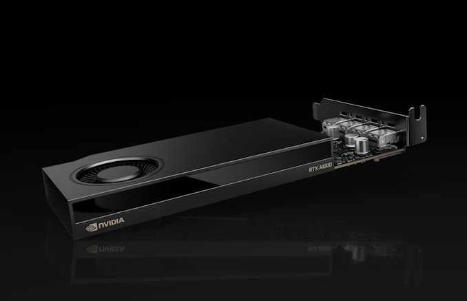
With NVIDIA’s Turing architecture turning six years old this year, the company has been retiring many of the remaining Turing products from its video card lineup. And today that spirit of spring cleaning is coming to the entry-level segment of NVIDIA’s professional visualization lineup, where NVIDIA is introducing a pair of new desktop cards based on their low-end Ampere hardware.
The new RTX A1000 and RTX A400 cards will be replacing the T1000/T600/T400 lineup, which was released three years ago in 2021. The new cards slot into the same entry-level category and finally finish fleshing out the RTX A series of proviz cards, offering NVIDIA’s Ampere-generation professional graphics technologies in the lowest-power, lowest-performance, lowest-cost configuration possible.
Notably, since the entry-level T-series were based on NVIDIA’s feature-limited TU11x silicon, which lacked ray tracing and tensor core support – the basis of NVIDIA’s RTX technologies and associated branding – this marks the first time these technologies will be available in NVIDIA’s entry-level desktop proviz cards. And accordingly, these are being promoted to RTX-branded video cards, ending the odd overlap with NVIDIA’s compute cards, which never carry RTX branding.
It goes without saying that as low-end cards, the ray tracing performance of either part is nothing to write home about, but it gives NVIDIA’s current proviz lineup a consistent set of graphics features from top to bottom.
| NVIDIA Professional Visualization Card Specification Comparison | ||||||
| A1000 | A400 | T1000 | T400 | |||
| CUDA Cores | 2304 | 768 | 896 | 384 | ||
| Tensor Cores | 72 | 24 | N/A | N/A | ||
| Boost Clock | 1460MHz | 1755MHz | 1395MHz | 1425MHz | ||
| Memory Clock | 12Gbps GDDR6 | 12Gbps GDDR6 | 10Gbps GDDR6 | 10Gbps GDDR6 |
||
| Memory Bus Width | 128-bit | 64-bit | 128-bit | 64-bit | ||
| VRAM | 8GB | 4GB | 8GB | 4GB | ||
| Single Precision | 6.74 TFLOPS | 2.7 TFLOPS | 2.5 TFLOPS | 1.09 TFLOPS | ||
| Tensor Performance | 53.8 TFLOPS | 21.7 TFLOPS | N/A | N/A | ||
| TDP | 50W | 50W | 50W | 30W | ||
| Cooling | Active, SS | Active, SS | Active, SS | Active, SS | ||
| Outputs | 4x mDP 1.4a | 4x mDP 1.4a | 3x mDP 1.4a | |||
| GPU | GA107 | TU117 | ||||
| Architecture | Ampere | Turing | ||||
| Manufacturing Process | Samsung 8nm | TSMC 12nm | ||||
| Launch Date | 04/2024 | 05/2024 | 05/2021 | 05/2021 | ||
Both the A1000 and A400 are based on the same board design, with NVIDIA doing away with any pretense of physical feature differentiation this time around (T400 was missing its 4th Mini DisplayPort). This means both cards are based on the GA107 GPU, sporting different core and memory configurations.
RTX A1000 is a not-quite-complete configuration of GA107, with 2304 CUDA cores and 72 tensor cores. This is paired with 8GB of GDDR6, which runs at 12Gbps, for a total of 192GB/second of memory bandwidth. The TDP of the card is 50 Watts, matching its predecessor.
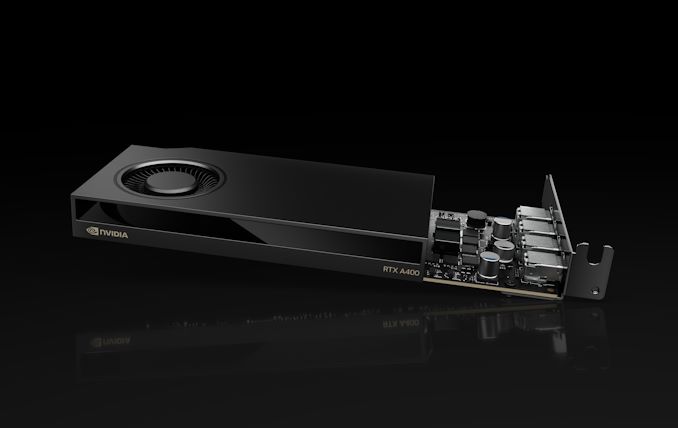
Meanwhile RTX A400 is far more cut down, offering about a third of the active hardware on the GPU itself, and half the memory bandwidth. On paper this gives it around 40% of T1000’s performance, and half the memory bandwidth – or 96GB/second. Notably, despite the hardware cut-down, the official TDP is still 50 Watts, versus the 30 Watts of its predecessor. So at this point NVIDIA will soon cease offering a desktop proviz card lower than 50 Watts.
As noted before, both cards otherwise feature the same physical design, with a half-height half-length (HHHL) board with active cooling. As you’d expect from such low-TDP cards, these are single-slot cooler designs. Both cards feature a quartet of Mini DisplayPorts, with the same DP 1.4a functionality that we’ve seen across all of NVIDIA’s products for the last several years.
Finally, video-focused users will want to make note that the A1000/A400 have slightly different video capabilities. While A1000 gets access to both of GA107’s NVDEC video decode blocks, A400 only gets access to a single block – one more cutback to differentiate the two cards. Otherwise, both video cards get access to the GPU’s sole NVENC block.
According to NVIDIA, the RTX A1000 will be available starting today through its distribution partners. Meanwhile the RTX A400 will hit distribution channels in May, and with OEMs expected to begin offering the cards as part of their pre-built systems this summer.
SK hynix is one of the few vertically integrated manufacturers in the flash-based storage market. The company is well-established in the OEM market. A few years back, they also started exploring direct end-user products. Internal SSDs (starting with the Gold S31 and Gold P31) were the first out of the door. Late last year, the company introduced the Beetle X31 portable SSD, its first direct-attached storage product. In February, a complementary product was introduced - the Tube T31 Stick SSD.
The Beetle X31 is a portable SSD with a Type-C upstream port and a separate cable. The Tube T31 is a take on the traditional thumb drive with a male Type-A interface. The size of the Beetle X31 makes the use of a bridge solution obvious. Our investigation into the Tube T31 also revealed the use of the same internal SSD, albeit with a different bridge. Read on for a detailed look at the Tube T31, including an analysis of its internals and evaluation of its performance consistency, power consumption, and thermal profile.
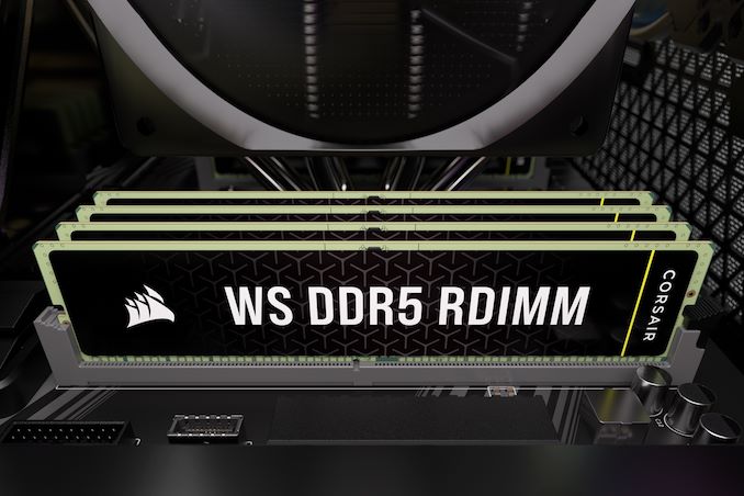
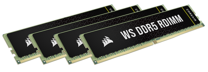
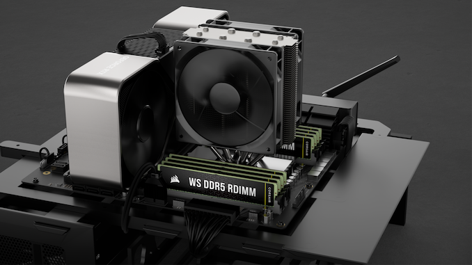
Corsair has introduced a family of registered memory modules with ECC that are designed for AMD's Ryzen Threadripper 7000 and Intel's Xeon W-2400/3400-series processors. The new Corsair WS DDR5 RDIMMs with AMD EXPO and Intel XMP 3.0 profiles will be available in kits of up to 256 GB capacity and at speeds of up to 6400 MT/s.
Corsair's family of WS DDR5 RDIMMs includes 16 GB modules operating at up to 6400 MT/s with CL32 latency as well as 32 GB modules functioning at 5600 MT/s with CL40 latency. At present, Corsair offers a quad-channel 64 GB kit (4×16GB, up to 6400 MT/s), a quad-channel 128GB kit (4×32GB, 5600 MT/s), an eight-channel 128 GB kit (8×16GB, 5600 MT/s), and an eight-channel 256 GB kit (8×32GB, 5600 MT/s) and it remains to be seen whether the company will expand the lineup.
Corsair's WS DDR5 RDIMMs are designed for AMD's TRX50 and WRX90 platforms as well as Intel's W790 platform and are therefore compatible with AMD's Ryzen Threadripper Pro 7000 and 7000WX-series as well as Intel's Xeon W-2400/3400-series CPUs. The modules feature both AMD EXPO and Intel XMP 3.0 profiles to easily set their beyond-JEDEC-spec settings and come with thin heat spreaders made of pyrolytic graphite sheet (PGS), which thermal conductivity than that of copper and aluminum of the same thickness. For now, Corsair does not disclose which RCD and memory chips its registered memory modules use.
Unlike many of its rivals among leading DIMM manufacturers, Corsair did not introduce its enthusiast-grade RDIMMs when AMD and Intel released their Ryzen Threadripper and Xeon W-series platforms for extreme workstations last year. It is hard to tell what the reason for that is, but perhaps the company wanted to gain experience working with modules featuring registered clock drivers (RCDs) as well as AMD's and Intel's platforms for extreme workstations.
The result of the delay looks to be quite rewarding: unlike modules from its competitors that either feature AMD EXPO or Intel XMP 3.0 profiles, Corsair's WS DDR5 RDIMMs come with both. While this may not be important on the DIY market where people know exactly what they are buying for their platform, this is a great feature for system integrators, which can use Corsair WS DDR5 RDIMMs both for their AMD Ryzen Threadripper and Intel Xeon W-series builds, something that greatly simplifies their inventory management.
Since Corsair's WS DDR5 RDIMMs are aimed at workstations and are tested to offer reliable performance beyond JEDEC specifications, they are quite expensive. The cheapest 64 GB DDR5-5600 CL40 kit costs $450, the fastest 64 GB DDR5-6400 CL32 kit is priced at $460, whereas the highest end 256 GB DDR5-5600 CL40 kit is priced at $1,290.
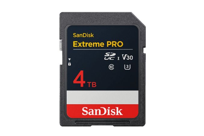
Western Digital this week is previewing the industry's first 4 TB SD card. The device is being showcased at the NAB trade show for broadcasters and content creators and will be released commercially in 2025.
Western Digital's SanDisk Extreme Pro SDUC 4 TB SD card complies with the Secure Digital Ultra Capacity standard (SDUC, which enables up to 128TB). The card uses the Ultra High Speed-I (UHS-I) interface and is rated for speed Class 10, therefore supporting a minimum speed of 10 MB/s and a maximum data transfer rate of 104 MB/s when working in UHS104 (SDR104) mode (there is a catch about performance, but more on that later). WD's SD card is also rated to meet Video Speed Class V30, supporting a minimal sequential write speed of 30 MB/s, which is believed to be good enough for 8K video recording, above and beyond the 4K video market that Western Digital is primarily aiming the forthcoming card at.
For now, Western Digital is not disclosing what NAND is in the SanDisk Extreme Pro SDUC 4 TB SD card. Given the high capacity and relatively distant 2025 release date, WD may be targetting this as one of their first products to use their forthcoming BiCS 9 NAND.
And while not listed in WD's official press release, we would be surprised if the forthcoming card didn't also support the off-spec DDR200/DDR208 mode, which allows for higher transfer rates than the UHS-I standard normally allows via double data rate signaling. Western Digital's current-generation SanDisk Extreme Pro SDXC 1 TB SD card already supports that mode, allowing it to reach read speeds as high as 170 MB/s, so it would be surprising to see the company drop it from newer products. That said, the catch with DDR208 remains the same as always: it's a proprietary mode that requires a compatible host to make use of.
Western Digital has not disclosed how much will its SanDisk Extreme Pro SDUC 4 TB SD card cost. A 1 TB SanDisk Extreme Pro card costs $140, so one can make guesses about the price of a 4 TB SD card that uses cutting-edge NAND.
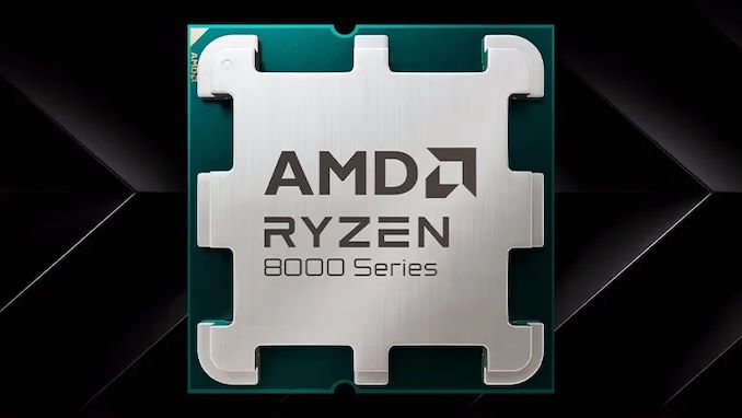
AMD has recently expanded its Ryzen 8000 series by introducing the Ryzen 7 8700F and Ryzen 5 8400F processors. Initially launched in China, these chips were added to AMD's global website, signaling they are available worldwide, apparently from April 1st. Built from the recent Zen 4-based Phoenix APUs using the TSMC 4nm node as their Zen 4 mobile chips, these new CPUs lack integrated graphics. However, the Ryzen 7 8700F does include the integrated Ryzen AI NPU for added capabilities in a world currently dominated by AI and moving it directly into the PC.
The company's decision to announce these chips in China aligns with its strategy to offer Ryzen solutions at every price point in the market. Although AMD didn't initially disclose the full specifications of these F-series models, and we did reach out to the company to ask about them, they refused to discuss them with us. Their listing on the website has now been updated with a complete list of specifications and features, with everything but the price mentioned.
| AMD Ryzen 8000G vs. Ryzen 8000F Series (Desktop) Zen 4 (Phoenix) |
|||||||||
| AnandTech | Cores/Threads | Base Freq |
Turbo Freq |
GPU | GPU Freq |
Ryzen AI (NPU) |
L3 Cache (MB) |
TDP | MSRP |
| Ryzen 7 | |||||||||
| Ryzen 7 8700G | 8/16 | 4200 | 5100 | R780M 12 CUs |
2900 | Y | 16 | 65W | $329 |
| Ryzen 7 8700F | 8/16 | 4100 | 5000 | - | - | Y | 16 | 65W | ? |
| Ryzen 5 | |||||||||
| Ryzen 5 8600G | 6/12 | 4300 | 5000 | R760M 8 CUs |
2800 | Y | 16 | 65W | $229 |
| Ryzen 5 8400F | 6/12 | 4200 | 4700 | - | - | N | 16 | 65W | ? |
The Ryzen 7 8700F features an 8C/16T design, with 16MB of L3 cache and the same 65W TDP as the Ryzen 7 8700G. Although the base clock speed is 4.1 GHz, it boosts to 5.0 GHz; this is 100 MHz less on both base/boost clocks than the 8700G. Meanwhile, the Ryzen 5 8400F is a slightly scaled-down version of the Ryzen 8600G APU, with 6C/12, 16MB of L3 cache, and again has a 100 MHz reduction to base clocks compared to the 8600G. Unlike the Ryzen 5 8400F, the Ryzen 7 8700F keeps AMD's Ryzen AI NPU, adding additional capability for generative AI.
The Ryzen 5 8400F can boost up to 4.7 GHz, 300 MHz slower than the Ryzen 5 8600G. AMD also allows overclocking for these new F-series chips, which means users could potentially boost the performance of these processors to match their G-series equivalents.
Pricing details are still pending, but to remain competitive, AMD will likely need to price these CPUs below the 8700G and 8600G, as well as the Ryzen 7 7700 and Ryzen 5 7600. These CPUs offer, albeit very limited, integrated graphics and have double the L3 cache capacity, along with higher boost clocks than the 8000F series chips, so pricing is something to consider whenever pricing becomes available.
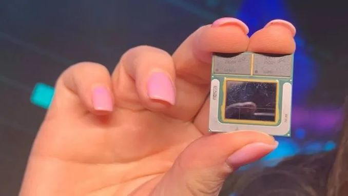
During the main keynote at Intel Vision 2024, Intel CEO Pat Gelsinger flashed a completed Lunar Lake chip off, much like EVP and General Manager of Intel's Client Computing Group (CCG) Michelle Johnston Holthaus did back at CES 2024. The contrast between the two glimpses of the Lunar Lake chip is that Pat Gelsinger gave us something juicier than just a photo op. He clarified and claimed the levels of AI performance we can expect to see when Lunar Lake launches.
According to Intel's CEO Pat Gelsinger, Lunar Lake, scheduled to be launched towards the end of this year, is set to raise the bar even further regarding on-chip AI capabilities and performance. At Intel's own Vision event, aptly named Intel Vision, current CEO of Intel Pat Gelsinger stated during his presentation that Lunar Lake will be the 'flagship SoC' for the next generation of AI PCs. Intel claims that Lunar Lake will have 3X the AI performance of their current Meteor Lake SoC, which is impressive as Meteor Lake is estimated to be running around 34 TOPS combined with the NPU, GPU, and CPU.
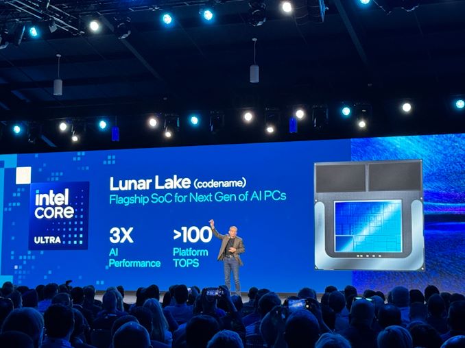
Factoring in the NPU within Meteor Lake, 11 of the 34 TOPS come solely from the NPU. Still, Intel claims that the NPU on Lunar Lake will hit a large 45 TOPs, akin to the Hailo-10 add-in card and similar to Qualcomm's Snapdragon X Elite processor. Factoring in the integrated graphics and the compute cores, Intel is claiming a combined total of over 100 TOPS, and with Microsoft's self-imposed guidelines of what constitutes an 'AI PC' coming in at 40 TOPS, Intel's NPU fits the bill.
Intel also alludes to how they are gaining a load of TOPS performance from the NPU, whether that be with new technologies; the NPU will likely be built in a more advanced node, perhaps Intel 18A. Another thing Intel didn't highlight was how they were measuring the TOPS performance, whether that be INT8 or INT4.
Still, one thing is clear: Intel wants to increase on-chip AI capabilities in desktop PCs and notebooks with each generation. Intel is also attempting to leverage more AI performance to help boost its goal to ship 100 million AI PCs by the end of 2025. Intel has already announced that it's shipped 5 million thus far and plans to sell another 40 million units by the end of the year.
One of the most significant talking points of the last six months in mobile computing has been Intel and their disaggregated Meteor Lake SoC architecture. Meteor Lake, along with the new Core and Core Ultra naming scheme, also heralds the dawn of their first tiled architecture for the mobile landscape on the latest Intel 4 node with Foveros packaging. In December last year, Intel unveiled their premier Meteor lake-based Core Ultra H series, with five SKUs ranging from two with 4P+8E+2LP/18T and three with 6P+8E+2LP/22T models. Since then, many vendors and manufacturers have launched notebooks capitalizing on Intel's latest multi-tiled Meteor Lake SoC architecture as the heart of power and performance, driving their latest models into 2024.
Today, we will focus on an attractive ultrabook via the ASUS Zenbook 14 OLED (UX3405MA), which features a thin and light design and is powered by Intel's latest Meteor Lake Core Ultra 7 155H processor. While much of the attention is going to come on how the Intel Core Ultra 7 155H with its 6P+8E+2LP/22T configuration and 8 Arc Xe integrated graphics cores will perform, the ASUS Zenbook 14 OLED UX3405MA has plenty of features within its sleek Ponder Blue colored shell to make it very interesting. Included is a 14" 3K (2880 x 1800) touchscreen OLED panel with a 120 Hz refresh rate, 32 GB of LPDDR5X memory (soldered), and a 1 TB NVMe M.2 SSD for storage.
In an unexpected move, Intel has announced plans to phase out the boxed versions of its enthusiasts-class 13th Generation Core 'Raptor Lake' processors. According to a product change notification (PCN) published by the company last month, Intel plans to stop shipping these desktop CPUs by late June. In its place will remain Intel's existing lineup of boxed 14th Generation Core processors, which are based on the same 'Raptor Lake' silicon and typically carry higher performance for similar prices.
Intel customers and distributors interested in getting boxed versions 13th Generation Core i5-13600K/KF, Core i7-13700K/KF, and Core i9-13900K/KF/KS 'Raptor Lake' processors with unlocked multiplier should place their orders by May 24, 2024. The company will ship these units by June 28, 2024. Meanwhile, the PCN does not mention any change to the availability of tray versions of these CPUs, which are sold to OEMs and wholesalers.
The impending discontinuation of Intel's boxed 13th Generation Core processors comes as the company's current 14th Generation product line, 'Raptor Lake Refresh' is largely a rehash of the same silicon at slightly higher clockspeeds. Case in point: all of the discontinued SKUs are based on Intel's B0 Raptor Lake silicon, which is still being used for their 14th Gen counterparts. So Intel has not discontinued producing any Raptor Lake silicon; only the number of retail SKUs is getting cut-down.
As outlined in our 14th Generation Core/Raptor Lake Refresh review, the 14th Gen chips largely make their 13th Gen counterparts redundant, offering better performance at every tier for the same list price. And with virtually all current generation motherboards supporting both generation of chips, apparently Intel feels there's little reason to keep around what's essentially older, slower SKUs of the same silicon.
Interestingly, the retirement of the enthusiast-class 13th Generation Core chips is coming before Intel discontinues their even older 12th Generation Core 'Alder Lake' processors. 12th Gen chips are still available to this day in both boxed and tray versions, and the Alder Lake silicon itself is still widely in use in multiple product families. So even though Alder Lake shares the same platform as Raptor Lake, the chips based on that silicon haven't been rendered redundant in the same way that 13th Gen Core chips have.
Ultimately, it would seem that Intel is intent on consolidating and simplifying its boxed retail chip offerings by retiring their near-duplicate SKUs. Which for PC buyers could present a minor opportunity for a deal, as retailers work to sell off their remaining 13th Gen enthusiast chips.
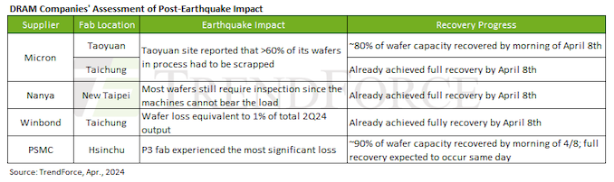
Following the magnitude 7.2 earthquake that struck Taiwan on April 3, 2024, there was immediate concern over what impact this could have on chip production within the country. Even for a well-prepared country like Taiwan, the tremor was the strongest quake to hit the region in 25 years, making it no small matter. But, according to research compiled by TrendForce, the impact on the production of DRAM will not be significant. The market tracking company believes that Taiwanese DRAM industry has remained largely unaffected, primarily due to their robust earthquake preparedness measures.
There are four memory makers in Taiwan: Micron, the sole member of the "big three" memory manufacturers on the island, runs two fabs. Meanwhile among the smaller players is Nanya (which has one fab), Winbond (which makes specialty memory at one fab), and PSMC (which produces specialty memory at one plant). The study found that these DRAM producers quickly resumed full operations, but had to throw away some wafers. The earthquake is estimated to have a minor effect on Q2 DRAM production, with a negligible 1% impact, TrendForce claims
In fact, as Micron is ramping up production of DRAM on its 1alpha and 1beta nm process technologies, it increases bit production of memory, which will positively affect supply of commodity DRAM in Q2 2025.
Following the earthquake, there was a temporary halt in quotations for both the contract and spot DRAM markets. However, the spot market quotations have already largely resumed, while contract prices have not fully restarted. Notably, Micron and Samsung ceased issuing quotes for mobile DRAM immediately after the earthquake, with no updates provided as of April 8th. In contrast, SK hynix resumed quotations for smartphone customers on the day of the earthquake and proposed more moderate price adjustments for Q2 mobile DRAM.
TrendForce anticipates a seasonal contract price increase for Q2 mobile DRAM of between 3% and 8%. This moderate increase is partly due to SK hynix's more restrained pricing strategy, which is likely to influence overall pricing strategies across the industry. The earthquake's impact on server DRAM primarily affected Micron's advanced fabrication nodes, potentially leading to a rise in final sale prices for Micron's server DRAM, according to TrendForce. However, the exact direction of future prices remains to be seen.
Meanwhile, DRAM fabs outside of Taiwan have none been directly affected by the quake. This includes Micron's HBM production line in Hiroshima, Japan, and Samsung's and SK hynix's HBM lines in South Korea, all of which are apparently operating with business as usual.
In general, the DRAM industry has shown resilience in the face of the earthquake, with minimal disruptions and a quick recovery. The abundant inventory levels for DDR4 and DDR5, coupled with weak demand, suggest that any slight price elevations caused by the earthquake are expected to normalize quickly. The only potential outlier here is DDR3, which is nearing the end of its commercial lifetime and production is already decreasing.
Google was among the first hyperscalers build custom silicon for its services, starting first with tensor processing units (TPUs) for its AI initiatives, and then video transcoding units (VCUs) for the YouTube service. But unlike its industry peers, the company has been slower to adopt custom CPU designs, prefering to stick to off-the-shelf chips from the major CPUs. This is finally changing at Google, with the announcement that the company has developed its own in-house datacenter CPU, the Axion.
Google's Axion processor is based on the Arm Neoverse V2 (Arm v9) platform, which is Arm's current-generation design for high-performance server CPUs, and is already employed in other chips such as NVIDIA's Grace and Amazon's Graviton4. Within Google, Axion is aimed at a wide variety of workloads, including web and app servers, data analytics, microservices, and AI training. Google claims that the Axion processors boast up to 50% higher performance and up to 60% better energy efficiency compared to current-generation x86-based processors, as well as offer a 30% higher performance compared to competing Arm-based CPUs for datacenters. Though as is increasingly common for the cryptic cloud side of Google's business, least for now the company isn't specifying what processors they're comparing Axion to in these metrics.
While Google is not disclosing core counts or the full specifications of its Axion CPUs, the company is revealing that they are incorporating their own secret sauce into the silicon in the form of the company's Titanium purpose-built microcontrollers. These microcontrollers are designed to handle basic operations like networking and security, as well as offload storage I/O processing to Hyperdisk block storage service. As a result of this offloading, virtually all of the CPU core resources should be available to actual workloads. As for the chip's memory subsystem, Axion uses conventional dual-rank DDR5 memory modules.
"Google's announcement of the new Axion CPU marks a significant milestone in delivering custom silicon that is optimized for Google's infrastructure, and built on our high-performance Arm Neoverse V2 platform," said Rene Haas, CEO of Arm. "Decades of ecosystem investment, combined with Google's ongoing innovation and open-source software contributions ensure the best experience for the workloads that matter most to customers running on Arm everywhere."
Google has previously deployed Arm-based processors for its own services, including BigTable, Spanner, BigQuery, and YouTube Ads and is ready to offer instances based on its Armv9-based Axion CPUs to its customers that can use software developed for Arm architectures.
Sources: Google, Wall Street Journal
Intel this morning is kicking off the second day of their Vision 2024 conference, the company’s annual closed-door business and customer-focused get-together. While Vision is not typically a hotbed for new silicon announcements from Intel – that’s more of an Innovation thing in the fall – attendees of this year’s show are not coming away empty handed. With a heavy focus on AI going on across the industry, Intel is using this year’s event to formally introduce the Gaudi 3 accelerator, the next-generation of Gaudi high-performance AI accelerators from Intel’s Habana Labs subsidiary.
The latest iteration of Gaudi will be launching in the third quarter of 2024, and Intel is already shipping samples to customers now. The hardware itself is something of a mixed bag in some respects (more on that in a second), but with 1835 TFLOPS of FP8 compute throughput, Intel believes it’s going to be more than enough to carve off a piece of the expansive (and expensive) AI market for themselves. Based on their internal benchmarks, the company expects to be able beat NVIDIA’s flagship Hx00 Hopper architecture accelerators in at least some critical large language models, which will open the door to Intel grabbing a larger piece of the AI accelerator market at a critical time in the industry, and a moment when there simply isn’t enough NVIDIA hardware to go around.
At Intel's Vision 2024 event, which is being held in Phoenix, AZ, has seen several key announcements. On the datacenter CPU front, Intel is using the show to unveil their newest branding for their venerable family of Xeon processors. Beginning with this year's sixth generation of processors, Intel is "evolving" the Xeon brand by retiring the "Xeon Scalable" branding in favor of Intel's new and simplified "Xeon 6" brand.
The Xeon 6 family is set to launch later this year with two primary variants: an all-performance (P) core chip codenamed Granite Rapids, and an all-efficiency (E) core chip codenamed Sierra Forest. Both of these chips will be sold under the Xeon 6 brand and sit on top of the same motherboard platform, with the Xeon 6 branding intended in part to underscore this shared platform. Though speaking of the chips themselves, at this time Intel isn't illustrating how the two sub-series of chips will be differentiated in terms of product numbers.
Over the last year, we've extensively covered Intel's Granite Rapids and Sierra Forest. For more information about Granite Rapids and Sierra Forest, here are some of our key pieces:
Intel debuted their Xeon Scalable branding in 2017 with the launch of the Xeon Platinum 8100 series, which was built using their Skylake microarchitecture. At the time Xeon Scalable replaced Intel's older Xeon E/EP/EX vX branding, resetting the generation count in the process.
Moving forward to 2024, Intel is looking to build an ecosystem befitting the current demands of technologies within key areas such as data centers, Edge, and the PC. Intel is laying the foundations for what it calls 'Intel Enterprise AI.' Using a vast array of frameworks and accelerators and working closely with partners, ISVs, and GSIs to create a large and open ecosystem, the newly branded Intel Xeon 6 platforms will be key in the enterprise market as we advance.
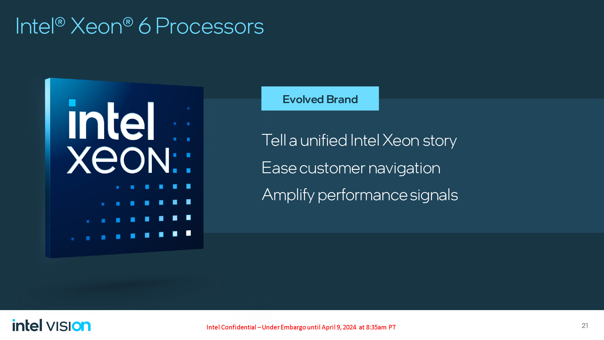
Intel has adopted a newer and simpler nomenclature for Granite Rapids and Sierra Forest, starting with the Intel Xeon 6 processors. Sierra Forest Xeon 6 processors are set to launch in Q2 of 2024, which include a chip featuring 288 E-cores. It will be the first product to adopt this new branding, which is designed to ease customer navigation between models. Meanwhile the Xeon 6 P-core Granite Rapids processors will come later.
Ultimately, the Xeon brand itself and what it entails (enterprise, workstation, server, and data center) isn't going anywhere. Instead, Intel is putting an increased focus on the generation number of the platform by moving it front and center, to more clearly highlight what generation of technology a part belongs to.
As mentioned, Intel's Xeon 6 processors, based on their Sierra Forest architecture, are set to launch in Q2 2024, while the Granite Rapids Xeon 6 platform is expected to come sometime in the second half of 2024.


TSMC has entered into a preliminary agreement with the U.S. Department of Commerce, securing up to $6.6 billion in direct funding and access to up to $5 billion in loans under the CHIPS and Science Act. With this latest round of support from the U.S. government, TSMC in turn will be adding a third fab to their Arizona project, with its investment in the region soaring to more than $65 billion. This move not only signifies the largest foreign direct investment in Arizona but also marks one of the biggest support packages that the U.S. government plans to make under the CHIPS Act, second only to Intel's $8.5 billion award last month.
TSMC is currently equipping its Fab 21 phase 1 and expects that it will start making chips using N4 and N5 (4 nm and 5 nm-class) process technologies in the first half of 2025. TSMC's Fab 21 phase 2 will commence operations in 2028, and will make chips on N3 and N2 (3 nm and 2 nm-class) production nodes. The newly-announced third fab (designation TBD) is set to manufacture chips on processes of 2 nm-class or beyond, with the start of production anticipated by the end of the decade.
TSMC has not announced a planned capacity for the new fab, only noting that it will be similar to the other two Arizona fabs, boasting a cleanroom space roughly twice as large as that of a typical "industry-standard logic fab." If it is sized similarly to the other Arizona fabs, then this strongly implies that the new fab will be another MegaFab-class facility – a mid-range fab producing around 25,000 wafer starts per month. TSMC does operate even larger fabs – the 100K WSPM GigaFab – though to date they've yet to build any of these outside of Taiwan.
“The CHIPS and Science Act provides TSMC the opportunity to make this unprecedented investment and to offer our foundry service of the most advanced manufacturing technologies in the United States,” said TSMC Chairman Dr. Mark Liu. “Our U.S. operations allow us to better support our U.S. customers, which include several of the world’s leading technology companies. Our U.S. operations will also expand our capability to trailblaze future advancements in semiconductor technology.”
The construction of three fabs in Arizona is poised to generate approximately 6,000 direct high-tech jobs, contributing significantly to the creation of a skilled workforce. This workforce is expected to play a crucial role in fostering a dynamic and competitive global semiconductor ecosystem. Moreover, the project is projected to create over 20,000 construction jobs, in addition to spawning tens of thousands of indirect jobs related to suppliers and consumer services.
AMD, Apple, and NVIDIA fully support TSMC's project and all of them expressed interest in using TSMC's capacities in the U.S.
“Today’s announcement highlights the strong commitment from Secretary Raimondo and the entire administration to ensure the U.S. plays a central role creating a more geographically diverse and resilient semiconductor supply chain,” said AMD Chair and CEO Lisa Su. “TSMC has a long track record of providing the leading-edge manufacturing capabilities that have enabled AMD to focus on what we do best, designing high-performance chips that change the world. We are committed to our partnership with TSMC and look forward to building our most advanced chips in U.S.”
TSMC's ventures in Arizona have encountered obstacles, such as setbacks caused by labor shortages and doubts about the U.S. governmental funding. As a result, production at the second facility has been postponed from 2026 to 2028. Moreover, Bloomberg has reported that at least one supplier for TSMC has called off its intended project in Arizona, attributing the decision to challenges in securing a workforce. The address the workforce issues, the TSMC grant includes a $50 million allocation for training of the local workforce.
In the arena of PC components, Be quiet! is a name synonymous with excellence, known for its fusion of silent functionality and exceptional performance. The company's broad range of products, from high-end power supply units (PSUs) to sophisticated cases and cooling solutions, including both air and liquid options, is crafted with a keen eye on reducing noise while maximizing efficiency. Be quiet! has earned accolades for its dedication to achieving near-silent operation across its lineup, making it a preferred choice among those in the PC enthusiast community who seek a serene computing environment. The diversity of its offerings reflects a deep understanding of the needs of tech enthusiasts and professionals alike, with each product designed to offer a blend of low noise levels and high efficiency.
Today we're looking at he Be quiet! Straight Power 12 750W PSU, a high-tier offering in Be quiet!'s PSU portfolio that exemplifies the brand's approach to product design. The Straight Power 12 series is engineered to deliver top performance and whisper-quiet operation, appealing to users who seek the optimal mix of power efficiency and sound level, without compromising on reliability and premium quality. The 750 Watt model that we are reviewing today is the weakest unit of the series, yet still enough to effortlessly power a modern gaming system with a mid-tier GPU.

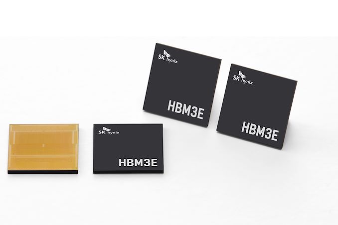
SK hynix this week announced plans to build its advanced memory packaging facility in West Lafayette, Indiana. The move can be considered as a milestone both for the memory maker and the U.S., as this is the first advanced memory packaging facility in the country and the company's first significant manufacturing operation in America. The facility will be used to build next-generation types of high-bandwidth memory (HBM) stacks when it begins operations in 2028. Also, SK hynix agreed to work on R&D projects with Purdue University.
"We are excited to become the first in the industry to build a state-of-the-art advanced packaging facility for AI products in the United States that will help strengthen supply-chain resilience and develop a local semiconductor ecosystem," said SK hynix CEO Kwak Noh-Jung.
The facility will handle assembly of HBM known good stacked dies (KGSDs), which consist of multiple memory devices stacked on a base die. Furthermore, it will be used to develop next-generations of HBM and will therefore house a packaging R&D line. However, the plant will not make DRAM dies themselves, and will likely source them from SK hynix's fabs in South Korea.
The plant will require SK hynix to invest $3.87 billion, which will make it one of the most advanced semiconductor packaging facilities in the world. Meanwhile, SK hynix held the investment agreement ceremony with representatives from Indiana State, Purdue University, and the U.S. government, which indicates parties financially involved in the project, but this week's event did not disclose whether SK hynix will receive any money from the U.S. government under the CHIPS Act or other funding initiatives.
The cost of the facility significantly exceeds that of packaging facilities built by other major players in the industry, such as ASE Group, Intel, and TSMC, which highlights how significant of an investment this is for SK hnix. In fact, $3.87 billion higher than advanced packaging CapEx budgets of Intel, TSMC and Samsung in 2023, based on estimates from Yole Intelligence.
Given that the fab comes online in 2028, based on SK hynix's product roadmap we'd expect that it will be used at least in part to assemble HBM4 and HBM4E stacks. Notably, since HBM4 and HBM4E stacks are set to feature a 2048-bit interface, their packaging process will be considerably more complex than the existing 1024-bit HBM3/HBM3E packaging and will require usage of more advanced tools, which is why it is poised to be more expensive than some existing advanced packaging facilities. Due to the extremely complex 2048-bit interface, many chip designers who are going to use HBM4/HBM4E are expected to integrate it directly onto their processors using hybrid bonding and not use silicon interposers. Unfortunately, it is unclear whether the SK hynix facility will be able to offer such service.
HBM is mainly used for AI and HPC applications, so it is strategically important to have its production in the U.S. Meanwhile, actual memory dies will still need to be made elsewhere, at dedicated DRAM fabs.
In addition to support set to be provided by state and local governmens, SK hynix chose to establish its new facility in West Lafayette, Indiana, to collaborate with Purdue University as well as with Purdue's Birck Nanotechnology Center on R&D projects, which includes advanced packaging and heterogeneous integration.
SK hynix intends to work in partnership with Purdue University and Ivy Tech Community College to create training programs and multidisciplinary degree courses aimed at nurturing a skilled workforce and establishing a consistent stream of emerging talent for its advanced memory packaging facility and R&D operations.
"SK hynix is the global pioneer and dominant market leader in memory chips for AI," Purdue University President Mung Chiang said. "This transformational investment reflects our state and university's tremendous strength in semiconductors, hardware AI, and hard tech corridor. It is also a monumental moment for completing the supply chain of digital economy in our country through chips advanced packaging. Located at Purdue Research Park, the largest facility of its kind at a U.S. university will grow and succeed through innovation."
PCI-SIG this week released version 0.5 of the PCI-Express 7.0 specification to its members. This is the second draft of the spec and the final call for PCI-SIG members to submit their new features to the standard. The latest update on the development of the specification comes a couple months shy of a year after the PCI-SIG published the initial Draft 0.3 specificaiton, with the PCI-SIG using the latest update to reiterate that development of the new standard remains on-track for a final release in 2025.
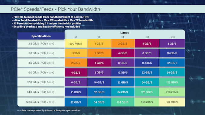
PCIe 7.0 is is the next generation interconnect technology for computers that is set to increase data transfer speeds to 128 GT/s per pin, doubling the 64 GT/s of PCIe 6.0 and quadrupling the 32 GT/s of PCIe 5.0. This would allow a 16-lane (x16) connection to support 256 GB/sec of bandwidth in each direction simultaneously, excluding encoding overhead. Such speeds will be handy for future datacenters as well as artificial intelligence and high-performance computing applications that will need even faster data transfer rates, including network data transfer rates.
To achieve its impressive data transfer rates, PCIe 7.0 doubles the bus frequency at the physical layer compared to PCIe 5.0 and 6.0. Otherwise, the standard retains pulse amplitude modulation with four level signaling (PAM4), 1b/1b FLIT mode encoding, and the forward error correction (FEC) technologies that are already used for PCIe 6.0. Otherwise, PCI-SIG says that the PCIe 7.0 speicification also focuses on enhanced channel parameters and reach as well as improved power efficiency.
Overall, the engineers behind the standard have their work cut out for them, given that PCIe 7.0 requires doubling the bus frequency at the physical layer, a major development that PCIe 6.0 sidestepped with PAM4 signaling. Nothing comes for free in regards to improving data signaling, and with PCIe 7.0, the PCI-SIG is arguably back to hard-mode development by needing to improve the physical layer once more – this time to enable it to run at around 30GHz. Though how much of this heavy lifting will be accomplished through smart signaling (and retimers) and how much will be accomplished through sheer materials improvements, such as thicker printed circuit boards (PCBs) and low-loss materials, remains to be seen.
The next major step for PCIe 7.0 is finalization of the version 0.7 of specification, which is considered the Complete Draft, where all aspects must be fully defined, and electrical specifications must be validated through test chips. After this iteration of the specification is released, no new features can be added. PCIe 6.0 eventually went through 4 major drafts – 0.3, 0.5, 0.7, and 0.9 – before finally being finalized, so PCIe 7.0 is likely on the same track.
Once finalized in 2025, it should take a few years for the first PCIe 7.0 hardware to hit the shelves. Although development work on controller IP and initial hardware is already underway, that process extends well beyond the release of the final PCIe specification.
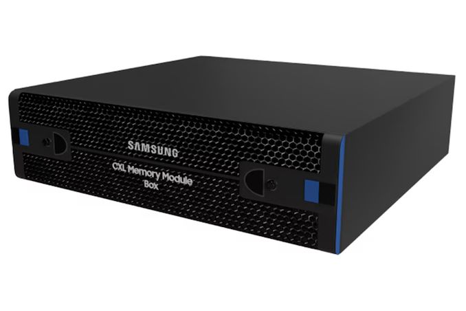
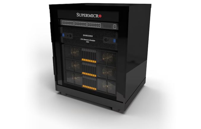
Composable disaggregated data center infrastructure promises to change the way data centers for modern workloads are built. However, to fully realize the potential of new technologies, such as CXL, the industry needs brand-new hardware. Recently, Samsung introduced its CXL Memory Module Box (CMM-B), a device that can house up to eight CXL Memory Module – DRAM (CMM-D) devices and add plenty of memory connected using a PCIe/CXL interface.
Samsung's CXL Memory Module Box (CMM-B) is the first device of this type to accommodate up to eight 2 TB E3.S CMM-D memory modules and add up to 16 TB of memory to up to three modern servers with appropriate connectors. As far as performance is concerned, the box can offer up to 60 GB/s of bandwidth (which aligns with what a PCIe 5.0 x16 interface offers) and 596 ns latency.
From a pure performance point of view, one CXL Memory Module—Box is slower than a dual-channel DDR5-4800 memory subsystem. Yet, the unit is still considerably faster than even advanced SSDs. At the same time, it provides very decent capacity, which is often just what the doctor ordered for many applications.
The Samsung CMM-B is compatible with the CXL 1.1 and CXL 2.0 protocols. It consists of a rack-scale memory bank (CMM-B), several application hosts, Samsung Cognos management console software, and a top-of-rack (ToR) switch. The device was developed in close collaboration with Supermicro, so expect this server maker to offer the product first.
Samsung's CXL Memory Module – Box is designed for applications that need a lot of memory, such as AI, data analytics, and in-memory databases, albeit not at all times. CMM-B allows the dynamic allocation of necessary memory to a system when it needs this memory and then uses DRAM with other machines. As a result, operators of datacenters can spend money on procuring expensive memory (16 TB of memory costs a lot), reduce power consumption, and add flexibility to their setups.
Rapidus, a Japan-based company developing 2nm process technology and aiming to commercialize it in 2027, will receive a huge government grant for its ongoing projects. The Japanese government will support Rapidus with subsidies totaling ¥590 billion yen ($3.89 billion). In addition to developing its 2nm production node and spending on cleanroom equipment, Rapidus will also fund the development of multi-chiplet packaging technology.
This extra funding will significantly help the company's ambitious plans. With the government's total support now at ¥920 billion ($6.068 billion), Rapidus is getting a solid push to become a significant player in the semiconductor industry. The whole project is expected to cost around ¥5 trillion ($32.983 billion), so the funding is not quite there yet. Meanwhile, the company may get enough financing with support from the Japanese government and large Japanese conglomerates like Toyota Motor and Nippon Telegraph and Telephone.
According to Atsuyoshi Koike, Rapidus's chief executive, the company is on track to start testing its production by April 2025 and aims to begin large-scale production by 2027. Commercial production of 2nm chips is set to commence sometime in 2025.
In addition to developing its 2nm fabrication process in collaboration with IBM and building its manufacturing facility, Rapidus is also working on advanced packaging technology for multi-chiplet system-in-packages (SiPs). The latest government subsidies include more than ¥50 billion ($329.85 million) for research and development in this area, the first time Japan has provided subsidies for such technologies.
It is noteworthy that Rapidus will use a section of Seiko Epson Corporation's Chitose Plant (located in Chitose City, Hokkaido) for its back-end packaging processes. This plant is near the company's fab, which is currently being built in Bibi World, an industrial park in Chitose City. This space will be dedicated to pilot-stage research and development activities.
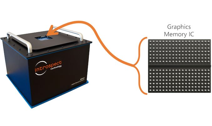
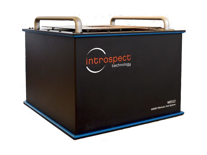
Introspect this week introduced its M5512 GDDR7 memory test system, which is designed for testing GDDR7 memory controllers, physical interface, and GDDR7 SGRAM chips. The tool will enable memory and processor manufacturers to verify that their products perform as specified by the standard.
One of the crucial phases of a processor design bring up is testing its standard interfaces, such as PCIe, DisplayPort, or GDDR is to ensure that they behave as specified both logically and electrically and achieve designated performance. Introspect's M5512 GDDR7 memory test system is designed to do just that: test new GDDR7 memory devices, troubleshoot protocol issues, assess signal integrity, and conduct comprehensive memory read/write stress tests.
The product will be quite useful for designers of GPUs/SoCs, graphics cards, PCs, network equipment and memory chips, which will speed up development of actual products that rely on GDDR7 memory. For now, GPU and SoC designers as well as memory makers use highly-custom setups consisting of many tools to characterize signal integrity as well as conduct detailed memory read/write functional stress testing, which are important things at this phase of development. But usage of a single tool greatly speeds up all the processes and gives a more comprehensive picture to specialists.
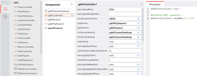
The M5512 GDDR7 Memory Test System is a desktop testing and measurement device that is equippped with 72 pins capable of functioning at up to 40 Gbps in PAM3 mode, as well as offering a virtual GDDR7 memory controller. The device features bidirectional circuitry for executing read and write operations, and every pin is equipped with an extensive range of analog characterization features, such as skew injection with femto-second resolution, voltage control with millivolt resolution, programmable jitter injection, and various eye margining features critical for AC characterization and conformance testing. Furthermore, the system integrates device power supplies with precise power sequencing and ramping controls, providing a comprehensive solution for both AC characterization and memory functional stress testing on any GDDR7 device.
Introspects M5512 has been designed in close collaboration with JEDEC members working on the GDDR7 specification, so it promises to meet all of their requirements for compliance testing. Notably, however, the device does not eliminate need for interoperability tests and still requires companies to develop their own test algorithms, but it's still a significant tool for bootstrapping device development and getting it to the point where chips can begin interop testing.
“In its quest to support the industry on GDDR7 deployment, Introspect Technology has worked tirelessly in the last few years with JEDEC members to develop the M5512 GDDR7 Memory Test System,” said Dr. Mohamed Hafed, CEO at Introspect Technology.
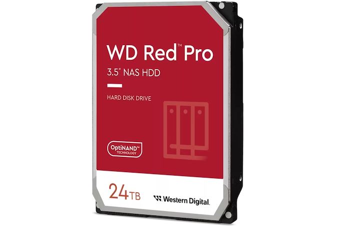
Nowadays highest-capacity hard drives are typically aimed at cloud service providers (CSPs) and enterprises, but this does not mean that creative professionals or regular users do not need them. To cater to demands of more regular consumers, Western Digital has started shipments of its Red Pro 24 TB HDDs, which are aimed at high-end NAS use for creative professionals with significant storage requirements.
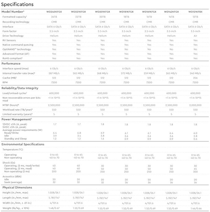
Western Digital's Red Pro 24 TB hard drives come approximately 20 months after their 22 TB model hit retail in 2022, offering an incremental improvement to WD's highest-capacity NAS and consumer hard drive offering. The platform uses conventional magnetic recording (CMR), feature a 7200 RPM rotating speed, are equipped with a 512 MB cache, and use OptiNAND technology to improve reliability as well as optimize performance and power consumption. The HDDs are rated for an up to 287 MB/s media to cache transfer rate, which makes them some of the fastest hard drives around (albeit, still a bit slower compared to CSP and enterprise-oriented HDDs).
Just like other high-end network-attached storage-aimed HDDs, the Red Pro 24 TB hard drives use helium-filled platforms that are very similar to those designed for enterprise drives. Consequently, the Red Pro 24 TB HDD are equipped with rotation vibration sensors to anticipate and proactively counteract disturbances caused by increased vibration and multi-axis shock sensors to detect subtle shock events and automatically offset them with dynamic fly height technology to ensure that heads to not scratch disks.
UPDATE 4/2/2024: Western Digital has notified us that WD Red Pro fully support ArmorCache capability, even though it is not listed in datasheets.
What these drives lack compared Apparently, just like WD Gold and Ultraster 22 TB and 24 TB drives for enterprises and cloud datacenters, WD Red Pro HDDs fully support the ArmorCache feature that provides protection against power loss when write-cache is enabled (WCE mode) and enhances performance when write-cache is disabled (WCD mode).
On the reliability side of matters, Western Digital's Red Pro 24 TB HDDs are designed for 24/7 operation in vibrating environments, such as enterprise-grade NAS with loads of bays, and are rated for up to 550 TB/year workloads as well as up to 600,000 load/unload cycles, which is in line with what Western Digital's WD Gold and Ultrastar hard drives offer.
As for power consumption, the WD Red Pro 24 TB consumes up to 6.4W during read and write operations, up to 3.9W in idle mode, and up to 1.2W in standby/sleep mode.
Western Digital's Red Pro 24 TB (WD240KFGX) HDDs are now shipping to resellers as well as NAS makers, and are slated to be available shortly. Expect these hard drives to be slightly cheaper than the WD Gold 24 TB model.
Typical CPU coolers do the job for standard heat management but often fall short when it comes to quiet operation and peak cooling effectiveness. This gap pushes enthusiasts and PC builders towards specialized aftermarket solutions designed for their unique demands. The premium aftermarket cooling niche is fiercely competitive, with brands vying to offer top-notch thermal management solutions.
Today we're shining a light on DeepCool's AK620 Digital cooler, a notable entry in the high-end CPU cooler arena. At first blush, the AK620 Digital stands out from the crowd mostly for its integrated LCD screen. Yet aesthetics aside, underneath the snappy screen is a tower cooler that was first and foremost engineered to exceed the cooling needs of the most powerful mainstream CPUs. And it's a big cooler at that: with a weight of 1.5Kg and 162mm tall, this is no lightweight heatsink and fan assembly. All of which helps to set it apart in a competitive marketplace.
Offering some rare insight into the scale of HBM memory sales – and on its growth in the face of unprecedented demand from AI accelerator vendors – the company recently disclosed that it expects HBM sales to make up "a double-digit percentage of its DRAM chip sales" this year. Which if it comes to pass, would represent a significant jump in sales for the high-bandwidth, high-priced memory.
As first reported by Reuters, SK hynix CEO Kwak Noh-Jung has commented that he expects HBM sales will constitute a double-digit percentage of its DRAM chip sales in 2024. This prediction corroborate with estimates from TrendForce, who believe that, industry-wide, HBM will account for 20.1% of DRAM revenue in 2024, more than doubling HBM's 8.4% revenue share in 2023.
And while SK hynix does not break down its DRAM revenue by memory type on a regular basis, a bit of extrapolation indicates that they're on track to take in billions in HBM revenue for 2024 – having likely already crossed the billion dollar mark itself in 2023. Last year, SK hynix's DRAM revenue $15.941 billion, according to Statista and TrendForce. So SK hynix only needs 12.5% of its 2024 revenues to come from HBM (assuming flat or positive revenue overall) in order to pass 2 billion in HBM sales. And even this is a low-ball estimate.
Overall, SK hynix currently commands about 50% of HBM market, having largely split the market with Samsung over the last couple of years. Given that share, and that DRAM industry revenue is expected to increase to $84.150 billion in 2024, SK hynix could earn as much as $8.45 billion on HBM in 2024 if TrendForce's estimates prove accurate.
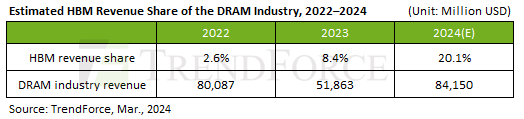
It should be noted that with demand for AI servers at record levels, all three leading makers of DRAM are poised to increase their HBM production capacity this year. Most notable here is a nearly-absent Micron, who was the first vendor to start shipping HBM3E memory to NVIDIA earlier this year. So SK hynix's near-majority of the HBM market may falter some this year, though with a growing pie they'll have little reason to complain. Ultimately, if sales of HBM reach $16.9 billion as projected, then all memory makers will be enjoying significant HBM revenue growth in the coming months.
Sources: Reuters, TrendForce
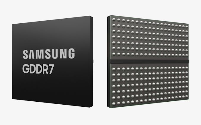
Now that JEDEC has published specification of GDDR7 memory, memory manufacturers are beginning to announce their initial products. The first out of the gate for this generation is Samsung, which has has quietly added its GDDR7 products to its official product catalog.
For now, Samsung lists two GDDR7 devices on its website: 16 Gbit chips rated for an up to 28 GT/s data transfer rate and a faster version running at up to 32 GT/s data transfer rate (which is in line with initial parts that Samsung announced in mid-2023). The chips feature a 512M x32 organization and come in a 266-pin FBGA packaging. The chips are already sampling, so Samsung's customers – GPU vendors, AI inference vendors, network product vendors, and the like – should already have GDDR7 chips in their labs.
The GDDR7 specification promises the maximum per-chip capacity of 64 Gbit (8 GB) and data transfer rates of 48 GT/s. Meanwhile, first generation GDDR7 chips (as announced so far) will feature a rather moderate capacity of 16 Gbit (2 GB) and a data transfer rate of up to 32 GT/s.
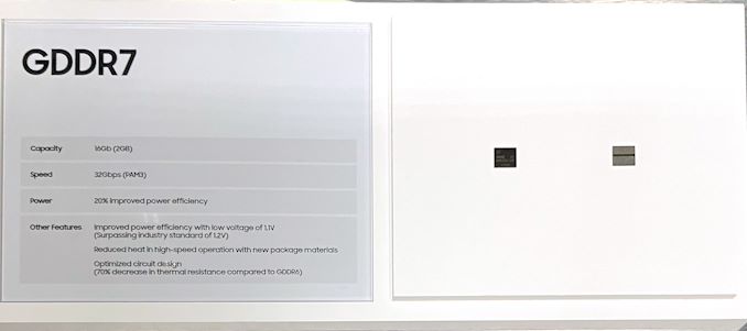
Performance-wise, the first generation of GDDR7 should provide a significant improvement in memory bandwidth over GDDR6 and GDDR6X. However capacity/density improvements will not come until memory manufacturers move to their next generation EUV-based process nodes. As a result, the first GDDR7-based graphics cards are unlikely to sport any memory capacity improvements. Though looking a bit farther down the road, Samsung and SK Hynix have previously told Tom's Hardware that they intend to reach mass production of 24 Gbit GDDR7 chips in 2025.
Otherwise, it is noteworthy that SK Hynix also demonstrated its GDDR7 chips at NVIDIA's GTC last week. So Samsung's competition should be close behind in delivering samples, and eventually mass production memory.
Source: Samsung (via @harukaze5719)
SK hynix is considering whether to build an advanced packaging facility in Indiana, reports the Wall Street Journal. If the company proceeds with the plan, it intends to invest $4 billion in it and construct one of the world's largest advanced packaging facilities. But to accomplish the project, SK hynix expects it will need help from the U.S. government.
Acknowledging the report but stopping short of confirming the company's plans, a company spokeswoman told the WSJ that SK hynix "is reviewing its advanced chip packaging investment in the U.S., but hasn’t made a final decision yet."
Companies like TSMC and Intel spend billions on advanced packaging facilities, but so far, no company has announced a chip packaging plant worth quite as much as SH hynix's $4 billion. The field of advanced packaging – CoWoS, passive silicon interposers, redistribution layers, die-to-die bonding, and other cutting edge technologies – has seen an explosion in demand in the last half-decade. As bandwidth advances with traditional organic packaging are largely played out, chip designers have needed to turn to more complex (and difficult to assemble) technologies in order to wire up an ever larger number of signals at ever-higher transfer rates. Which has turned advanced packaging into a bottleneck for high-end chip and accelerator production, driving a need for additional packaging facilities.
If SK hynix approves the project, the advanced packaging facility is expected to begin operations in 2028 and could create as many as 1,000 jobs. With an estimated cost of $4 billion, the plant is poised to become one of the largest advanced packaging facilities in the world.
Meanwhile, government backing is thought to be essential for investments of this scale, with potential state and federal tax incentives, according to the report. These incentives form part of a broader initiative to bolster the U.S. semiconductor industry and decrease dependence on memory produced in South Korea.
SK hynix is the world's leading producer of HBM memory, and is one of the key HBM suppliers to NVIDIA. Next generations of HBM memory (including HBM4 and HBM4E) will require even closer collaboration between chip designers, chipmakers, and memory makers. Therefore, packaging HBM in America could be a significant benefit for NVIDIA, AMD, and other U.S. chipmakers.
Investing in the Indiana facility will be a strategic move by SK hynix to enhance its advanced chip packaging capabilities in general and demonstrating dedication to the U.S. semiconductor industry.

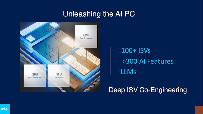
Today, Intel announced that it is looking to progress its AI PC Acceleration program further by offering various new toolkits and devkits designed for software and hardware AI developers under a new AI PC Developer Program sub-initiative. Originally launched on October 23, the AI PC Acceleration program was created to connect hardware vendors with software developers, using Intel's vast resources and experience to develop a broader ecosystem as the world pivots to one driven by AI development.
Intel aims to maximize the potential of AI applications and software and broaden the whole AI-focused PC ecosystem by aiming for AI within 100 million Intel-driven AI PCs by 2025. The AI PC Developer Program aims to simplify the adoption of new AI technologies and frameworks on a larger scale. It provides access to various tools, workflows, AI-deployment frameworks, and developer kits, allowing developers to take advantage of the latest NPU found within Intel's Meteor Lake Core Ultra series of processors.
It also offers centralized resources like toolkits, documentation, and training to allow developers to fully utilize their software and hardware in tandem with the technologies associated with Meteor Lake (and beyond) to enhance AI and machine learning application performance. Such toolkits are already broadly used by developers, including Intel's open-source OpenVino.
Furthermore, this centralized resource platform is designed to streamline the AI development process, making it more efficient and effective for developers to integrate AI capabilities into their applications. It is designed to play a crucial role in Intel’s strategy to not only advance AI technology but also to make it more user-friendly and adaptable to various real-world applications.
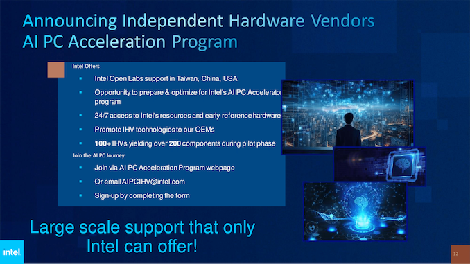
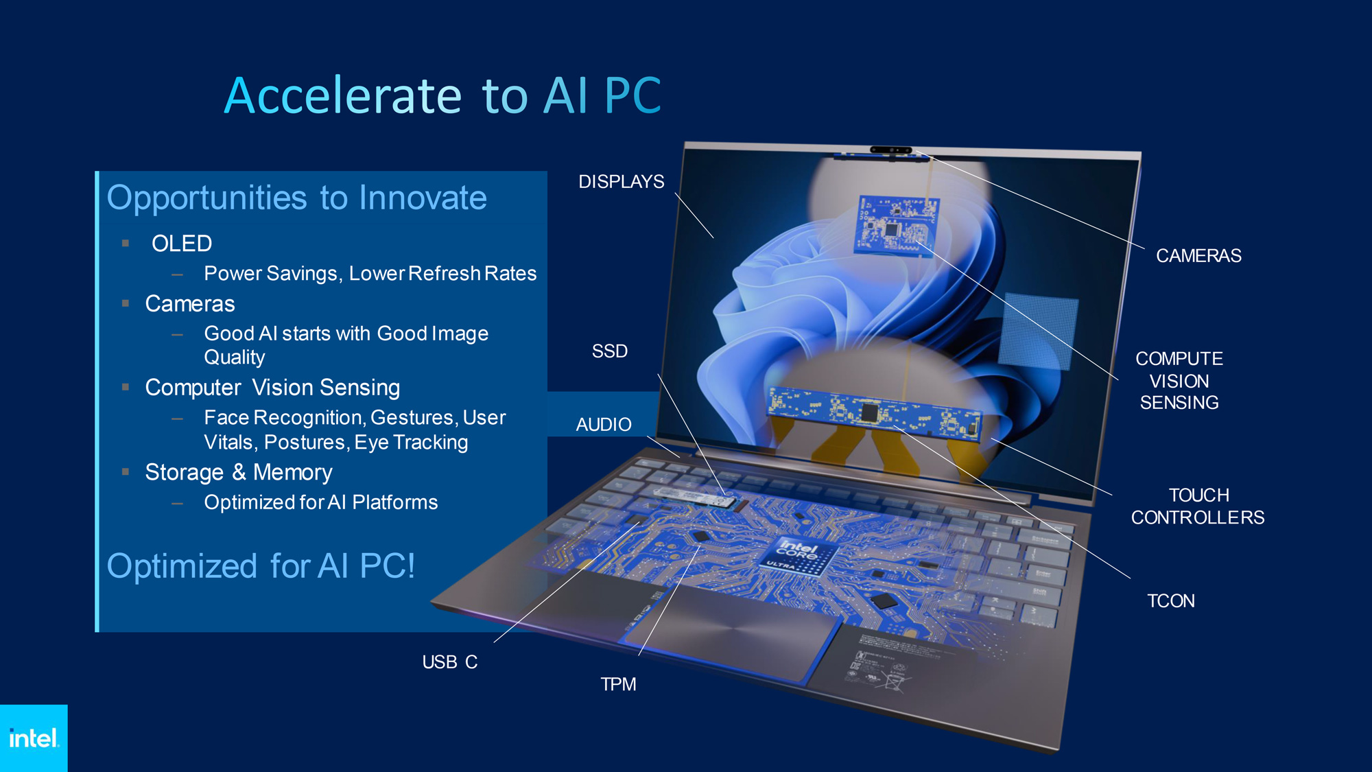
Notably, this is both a software and a hardware play. Intel isn't just looking to court more software developers to utilize their AI resources, but they also want to get independent hardware vendors (IHVs) on board. OEMs and system assemblers are largely already covered under Microsoft's requirements for Windows certification, but Intel wants to get the individual parts vendors involved as well. How can AI be used to improve audio performance? Display performance? Storage performance? That's something that Intel wants to find out.
"We have made great strides with our AI PC Acceleration Program by working with the ecosystem. Today, with the addition of the AI PC Developer Program, we are expanding our reach to go beyond large ISVs and engage with small and medium sized players and aspiring developers" said Carla Rodriguez, Vice President and General Manager of Client Software Ecosystem Enabling. "Our goal is to drive a frictionless experience by offering a broad set of tools including the new AI-ready Developer Kit,"
The Intel AI PC Acceleration Program offers 24/7 access to resources and early reference hardware so that both ISVs and software developers can create and optimize workloads before launching retail components. Developers can join the AI PC Acceleration Program at their official webpage or email AIPCIHV@intel.com for further information
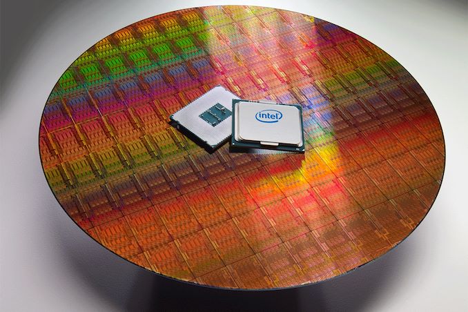
China has initiated a policy shift to eliminate American processors from government computers and servers, reports Financial Times. The decision is aimed to gradually eliminate processors from AMD and Intel from system used by China's government agencies, which will mean lower sales for U.S.-based chipmakers and higher sales of China's own CPUs.
The new procurement guidelines, introduced quietly at the end of 2023, mandates government entities to prioritize 'safe and reliable' processors and operating systems in their purchases. This directive is part of a concerted effort to bolster domestic technology and parallels a similar push within state-owned enterprises to embrace technology designed in China.
The list of approved processors and operating systems, published by China's Information Technology Security Evaluation Center, exclusively features Chinese companies. There are 18 approved processors that use a mix of architectures, including x86 and ARM, while the operating systems are based on open-source Linux software. Notably, the list includes chips from Huawei and Phytium, both of which are on the U.S. export blacklist.
This shift towards domestic technology is a cornerstone of China's national strategy for technological autonomy in the military, government, and state sectors. The guidelines provide clear and detailed instructions for exclusively using Chinese processors, marking a significant step in China's quest for self-reliance in technology.
State-owned enterprises have been instructed to complete their transition to domestic CPUs by 2027. Meanwhile, Chinese government entites have to submit progress reports on their IT system overhauls quarterly. Although some foreign technology will still be permitted, the emphasis is clearly on adopting local alternatives.
The move away from foreign hardware is expected to have a measurable impact on American tech companies. China is a major market for AMD (accounting for 15% of sales last year) and Intel (commanding 27% of Intel's revenue), contributing to a substantial portion of their sales. Additionally, Microsoft, while not disclosing specific figures, has acknowledged that China accounts for a small percentage of its revenues. And while government sales are only a fraction of overall China sales (as compared to the larger commercial PC business) the Chinese government is by no means a small customer.
Analysts questioned by Financial Times predict that the transition to domestic processors will advance more swiftly for server processors than for client PCs, due to the less complex software ecosystem needing replacement. They estimate that China will need to invest approximately $91 billion from 2023 to 2027 to overhaul the IT infrastructure in government and adjascent industries.
DeepCool is one of the few veterans in the PC power & cooling components field still active today. The Chinese company was first founded in 1996 and initially produced only coolers and cooling accessories, but quickly diversified into the PC Case and power supply unit (PSU) markets. To this day, DeepCool stays almost entirely focused on PC power & cooling products, with input devices and mousepads being their latest diversification attempt.
Today's review turns the spotlight toward DeepCool’s PSUs and, more specifically, the PX850G 850W ATX 3.0 PSU, which currently is their most popular power supply. The PX850G is engineered to balance all-around performance with reliability and cost, all while providing ATX 3.0 compliance. It is based on a highly popular high-output platform but, strangely, DeepCool rated the PX850G for operation up to 40°C.

When a major industry slowdown occurs, big companies tend to slowdown their mid-term and long-term capacity related investments. This is exactly what happened to SK hynix's Yongin Semiconductor Cluster, a major project announced in April 2021 and valued at $106 billion. While development of the site has been largely completed, only 35% of the initial shell building has been constructed, according to the Korean Ministry of Trade, Industry, and Energy.
"Approximately 35% of Fab 1 has been completed so far and site renovation is in smooth progress," a statement by the Korean Ministry of Trade, Industry, and Energy reads. "By 2046, over KRW 120 trillion ($90 billion today, $106 billion in 2021) in investment will be poured to complete Fabs 1 through 4, and construction of Fab 1's production line will commence in March next year. Once completed, the infrastructure will rank as the world's largest three-story fab."
The new semiconductor fabrication cluster by SK hynix announced almost exactly three years ago is primarily meant to be used to make DRAM for PCs, mobile devices, and servers using advanced extreme ultraviolet lithography (EUV) process technologies. The cluster, located near Yongin, South Korea, is intended to consist of four large fabs situated on a 4.15 million m2 site. With a planned capacity of approximately 800,000 wafer starts per month (WSPMs), it is set to be one of the world's largest semiconductor production hubs.
With that said, SK hynix's construction progress has been slower than the company first projected. The first fab in the complex was originally meant to come online in 2025, with construction starting in the fourth quarter of 2021. However, SK hynix began to cut its capital expenditures in the second half of 2022, and the Yongin Semiconductor Cluster project fell a victim of that cut. To be sure, the site continues to be developed, just at a slower pace; which is why some 35% of the first fab shell has been built at this point.
If completed as planned in 2021, the first phase of SK hynix Yongin operations would have been a major memory production facility costing $25 billion, equipped with EUV tools, and capable of 200,000-WSPM, according to reports from 2021.
Sources: Korean Ministry of Trade, Industry, and Energy; ComputerBase
Micron this week announced that it had begun sampling of its 256 GB multiplexer combined (MCR) DIMMs, the company's highest-capacity memory modules to date. These brand-new DDR5-based MCRDIMMs are aimed at next-generation servers, particularly those powered by Intel's Xeon Scalable 'Granite Rapids' processors that are set to support 12 or 24 memory slots per socket. Usage of these modules can enable datacenter machines with 3 TB or 6 TB of memory, with the combined ranks allowing for effect data rates of DDR5-8800.
"We also started sampling our 256 GB MCRDIMM module, which further enhances performance and increases DRAM content per server," said Sanjay Mehrotra, chief executive of Micron, in prepared remarks for the company's earnings call this week.
In addition to announcing sampling of these modules, Micron also demonstrated them at NVIDIA's GTC conference, where server vendors and customers alike are abuzz at building new servers for the next generation of AI accelerators. Our colleagues from Tom's Hardware have managed to grab a couple of pictures of Micron's 256 GB DDR5-8800 MCR DIMMs.
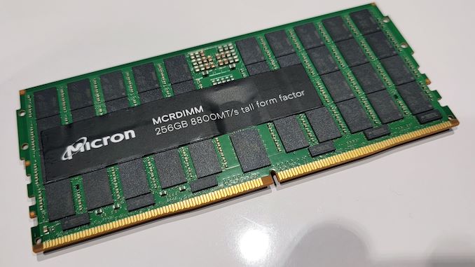
Image Credit: Tom's Hardware
Apparently, Micron's 256 GB DDR5-8800 MCRDIMMs come in two variants: a taller module with 80 DRAM chips distributed on both sides, and a standard-height module using 2Hi stacked packages. Both are based on monolithic 32 Gb DDR5 ICs and are engineered to cater to different server configurations with the standard-height MCRDIMM adressing 1U servers.The taller version consumes about 20W of power, which is in line with expectations as a 128 GB DDR5-8000 RDIMM consumes around 10W in DDR5-4800 mode. I have no idea about power consumption of the version that uses 2Hi packages, though expect it to be a little bit hotter and harder to cool down.
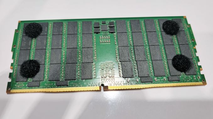
Image Credit: Tom's Hardware
Multiplexer Combined Ranks (MCR) DIMMs are dual-rank memory modules featuring a specialized buffer that allows both ranks to operate simultaneously. This buffer enables the two physical ranks to operate as though they were separate modules working in parallel, which allows for concurrent retrieval of 128 bytes of data from both ranks per clock cycle (compared to 64 bytes per cycle when it comes to regular memory modules), effectively doubling performance of a single module. Of course, since the modules retains physical interface of standard DDR5 modules (i.e., 72-bits), the buffer works with host at a very high data transfer rate to transfer that fetched data to the host CPU. These speeds exceed the standard DDR5 specifications, reaching 8800 MT/s in this case.
While MCR DIMMs make memory modules slightly more complex than regular RDIMMs, they increase performance and capacity of memory subsystem without increasing the number of memory modules involved, which makes it easier to build server motherboards. These modules are poised to play a crucial role in enabling the next generation of servers to handle increasingly demanding applications, particularly in the AI field.
Sources: Tom's Hardware, Micron
Being the first company to ship HBM3E memory has its perks for Micron, as the company has revealed that is has managed to sell out the entire supply of its advanced high-bandwidth memory for 2024, while most of their 2025 production has been allocated, as well. Micron's HBM3E memory (or how Micron alternatively calls it, HBM3 Gen2) was one of the first to be qualified for NVIDIA's updated H200/GH200 accelerators, so it looks like the DRAM maker will be a key supplier to the green company.
"Our HBM is sold out for calendar 2024, and the overwhelming majority of our 2025 supply has already been allocated," said Sanjay Mehrotra, chief executive of Micron, in prepared remarks for the company's earnings call this week. "We continue to expect HBM bit share equivalent to our overall DRAM bit share sometime in calendar 2025."
Micron's first HBM3E product is an 8-Hi 24 GB stack with a 1024-bit interface, 9.2 GT/s data transfer rate, and a total bandwidth of 1.2 TB/s. NVIDIA's H200 accelerator for artificial intelligence and high-performance computing will use six of these cubes, providing a total of 141 GB of accessible high-bandwidth memory.
"We are on track to generate several hundred million dollars of revenue from HBM in fiscal 2024 and expect HBM revenues to be accretive to our DRAM and overall gross margins starting in the fiscal third quarter," said Mehrotra.
The company has also began sampling its 12-Hi 36 GB stacks that offer a 50% more capacity. These KGSDs will ramp in 2025 and will be used for next generations of AI products. Meanwhile, it does not look like NVIDIA's B100 and B200 are going to use 36 GB HBM3E stacks, at least initially.
Demand for artificial intelligence servers set records last year, and it looks like it is going to remain high this year as well. Some analysts believe that NVIDIA's A100 and H100 processors (as well as their various derivatives) commanded as much as 80% of the entire AI processor market in 2023. And while this year NVIDIA will face tougher competition from AMD, AWS, D-Matrix, Intel, Tenstorrent, and other companies on the inference front, it looks like NVIDIA's H200 will still be the processor of choice for AI training, especially for big players like Meta and Microsoft, who already run fleets consisting of hundreds of thousands of NVIDIA accelerators. With that in mind, being a primary supplier of HBM3E for NVIDIA's H200 is a big deal for Micron as it enables it to finally capture a sizeable chunk of the HBM market, which is currently dominated by SK Hynix and Samsung, and where Micron controlled only about 10% as of last year.
Meanwhile, since every DRAM device inside an HBM stack has a wide interface, it is physically bigger than regular DDR4 or DDR5 ICs. As a result, the ramp of HBM3E memory will affect bit supply of commodity DRAMs from Micron, the company said.
"The ramp of HBM production will constrain supply growth in non-HBM products," Mehrotra said. "Industrywide, HBM3E consumes approximately three times the wafer supply as DDR5 to produce a given number of bits in the same technology node."
MediaTek this week has introduced a new lineup of Dimensity Auto Cockpit system-on-chips, covering the entire market spectrum from entry-level to premium. And while automotive chip announcements are admittedly not normally the most interesting of things, this one is going to be an exception to that rule because of whose graphics IP MediaTek is tapping for the chips: NVIDIA's. This means the upcoming Dimensity Auto Cockpit chips will be the first chips to be released by a third-party (non-NVIDIA) vendor to be based around NVIDIA's GeForce graphics technology.
NVIDIA's first attempt to license its GPU IP to third parties dates back to the year 2013, when the company proposed to license its Kepler GPU IP and thus rival Arm and Imagination Technologies. An effort that, at the time, landed flat on its face. But over a decade later and a fresh effort at hand to license out some of NVIDIA's IP, and it seems NVIDIA has finally succeeded. Altogether, MediaTek's new Dimensity Auto Cockpit system-on-chips will rely on NVIDIA's GPU IP, Drive OS, and CUDA, setting a historical development for both companies.
MediaTek's family of next-generation Dimensity Auto Cockpit processors consists of four distinct system-on-chip, including CX-1 for range-topping vehicles, CY-1, CM-1, and CV-1 for entry-level cars. These are highly-integrated SoCs packing Armv9-A-based general-purpose CPU cores as well as NVIDIA's next-generation graphics processing unit IP. NVIDIA's GPU IP can run AI workloads for driver assistance as well as power infotainment system, as it fully supports such graphics technologies like real-time ray-tracing and DLSS 3 image upscaling.
The Dimensity Auto Cockpit processors are monolithic SoCs with built-in multi-camera HDR ISP, according to HardwareLuxx. This ISP supports front-facing, in-cabin, and bird's-eye-view cameras for a variety of safety applications. Additionally, these processors feature an audio DSP that supports various voice assistants.
The announcement from MediaTek does not disclose which generation of NVIDIA's graphics IP they're adopting – only that it's a "next-gen" design. Given the certification requirements involved, automotive SoC announcements tend to be rather conservative, so it remains to be seen just how "next gen" this graphics IP will actually be compared to the current generation Ada Lovelace architecture.
The new MediaTek SoCs will be fully supported by NVIDIA's Drive OS, which is widely used by automakers already. This will allow automakers to unify their software stack and use the same set of software for all of their cars powered by MediaTek's Dimensity. Furthermore, since NVIDIA's Drive OS fully supports CUDA, TensorRT, and Nsight, MediaTek's Dimensity SoCs will be able to take advantage of AI applications developed for the green company's platform.
“Generative AI is transforming the automotive industry in the same way that it has revolutionized the mobile market with more personalized and intuitive computing experiences,” said Jerry Yu, Corporate Senior Vice President and General Manager of MediaTek’s CCM Business Group. “The Dimensity Auto Cockpit portfolio will unleash a new wave of AI-powered entertainment in vehicles, and our unified hardware and software platform makes it easy for automakers to scale AI capabilities across their entire lineup.”
Without a doubt, licensing graphics IP and platform IP to a third party marks a milestone for NVIDIA in general, as well as its automotive efforts in particular. Leveraging DriveOS and CUDA beyond NVIDIA's own hardware platform is a big deal for a business unit that NVIDIA has long considered poised for significant growth, but has faced stiff competition and a slow adoption rate thanks to conservative automakers. Meanwhile, what remains to be seen is how MediaTek's new Dimensity Auto Cockpit processors will stack up against NVIDIA's own previously announced Thor SoC and associated DRIVE Thor platform, which integrates a Blackwell-based GPU delivering 800 TFLOPS of 8-bit floating point AI performance.
AMD's FidelityFX Super Resolution 3 technology package introduced a plethora of enhancements to the FSR technology on Radeon RX 6000 and 7000-series graphics cards last September. But perfection has no limits, so this week, the company is rolling out its FSR 3.1 technology, which improves upscaling quality, decouples frame generation from AMD's upscaling, and makes it easier for developers to work with FSR.
Arguably, AMD's FSR 3.1's primary enhancement is its improved temporal upscaling image quality: compared to FSR 2.2, the image flickers less at rest and no longer ghosts when in movement. This is a significant improvement, as flickering and ghosting artifacts are particularly annoying. Meanwhile, FSR 3.1 has to be implemented by the game developer itself, and the first title to support this new technology sometime later this year is Ratchet & Clank: Rift Apart.
| Temporal Stability | |
|
|
|
| AMD FSR 2.2 | AMD FSR 3.1 |
| Ghosting Reduction | |
|
|
|
| AMD FSR 2.2 | AMD FSR 3.1 |
Another significant development brought by FSR 3.1 is its decoupling from the Frame Generation feature introduced by FSR 3. This capability relies on a form of AMD's Fluid Motion Frames (AFMF) optical flow interpolation. It uses temporal game data like motion vectors to add an additional frame between existing ones. This ability can lead to a performance boost of up to two times in compatible games, but it was initially tied to FSR 3 upscaling, which is a limitation. Starting from FSR 3.1, it will work with other upscaling methods, though AMD refrains from saying which methods and on which hardware for now. Also, the company does not disclose when it is expected to be implemented by game developers.
In addition, AMD is bringing support for FSR3 to Vulkan and Xbox Game Development Kit, enabling game developers on these platforms to use it. It also adds FSR 3.1 to the FidelityFX API, which simplifies debugging and enables forward compatibility with updated versions of FSR.
Upon its release in September 2023, AMD FSR 3 was initially supported by two titles, Forspoken and Immortals of Aveum, with ten more games poised to join them back then. Fast forward to six months later, the lineup has expanded to an impressive roster of 40 games either currently supporting or set to incorporate FSR 3 shortly. As of March 2024, FSR is supported by games like Avatar: Frontiers of Pandora, Starfield, The Last of Us Part I. Shortly, Cyberpunk 2077, Dying Light 2 Stay Human, Frostpunk 2, and Ratchet & Clank: Rift Apart will support FSR shortly.
Source: AMD
The Ultra Ethernet Consortium (UEC) has announced this week that the next-generation interconnection consortium has grown to 55 members. And as the group works towards developing the initial version of their ultra-fast Ethernet standard, they have released some of the first technical details on the upcoming standard.
Formed in the summer of 2023, the UEC aims to develop a new standard for interconnection for AI and HPC datacenter needs, serving as a de-facto (if not de-jure) alternative to InfiniBand, which is largely under the control of NVIDIA these days. The UEC began to accept new members back in November, and just in five months' time it gained 45 new members, which highlights massive interest for the new technology. The consortium now boasts 55 members and 715 industry experts, who are working across eight technical groups.
There is a lot of work at hand for the UEC, as the group has laid out in their latest development blog post, as the consortium works to to build a unified Ethernet-based communication stack for high-performance networking supporting artificial intelligence and high-performance computing clusters. The consortium's technical objectives include developing specifications, APIs, and source code for Ultra Ethernet communications, updating existing protocols, and introducing new mechanisms for telemetry, signaling, security, and congestion management. In particular, Ultra Ethernet introduces the UEC Transport (UET) for higher network utilization and lower tail latency to speed up RDMA (Remote Direct Memory Access) operation over Ethernet. Key features include multi-path packet spraying, flexible ordering, and advanced congestion control, ensuring efficient and reliable data transfer.
These enhancements are designed to address the needs of large AI and HPC clusters — with separate profiles for each type of deployment — though everything is done in a surgical manner to enhance the technology, but reuse as much of the existing Ethernet as possible to maintain cost efficiency and interoperability.
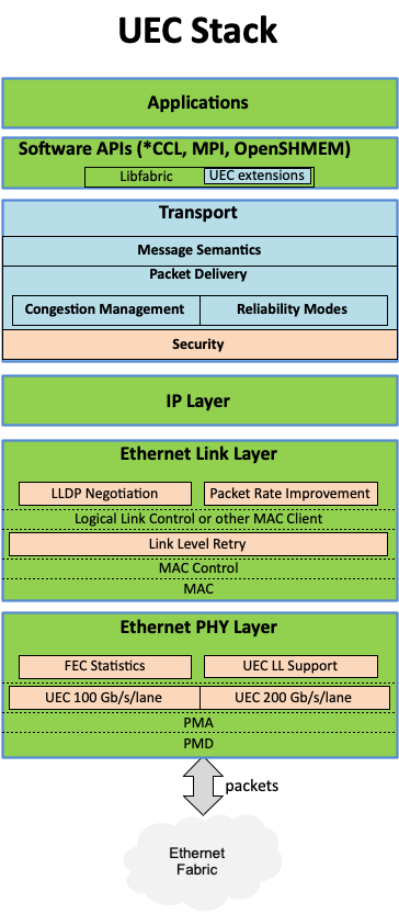
The consortium's founding members include AMD, Arista, Broadcom, Cisco, Eviden (an Atos Business), HPE, Intel, Meta, and Microsoft. After the Ultra Ethernet Consortium (UEC) began to accept new members in October, 2023, numerous industry heavyweights have joined the group, including Baidu, Dell, Huawei, IBM, Nokia, Lenovo, Supermicro, and Tencent.
The consortium currently plans to release the initial 1.0 version of the UEC specification publicly sometime in the third quarter of 2024.
"There was always a recognition that UEC was meeting a need in the industry," said J Metz, Chair of the UEC Steering Committee. "There is a strong desire to have an open, accessible, Ethernet-based network specifically designed to accommodate AI and HPC workload requirements. This level of involvement is encouraging; it helps us achieve the goal of broad interoperability and stability."
While it is evident that then Ultra Ethernet Consortium is gaining support across the industry, it is still unclear where other industry behemoths like AWS and Google stand. While the hardware companies involved can design Ultra Ethernet support into their hardware and systems, the technology ultimately exists to serve large datacenter and HPC system operators. So it will be interesting to see what interest they take in (and how quickly they adopt) the nascent Ethernet backbone technology once hardware incorporating it is ready.
Proving the adage “ask, and you shall receive”, Qualcomm is back this week for a second Snapdragon SoC announcement for mobile phones. This time, the company is announcing the Snapdragon 7+ Gen 3, the latest-generation member of their relatively new Snapdragon 7+ lineup of SoCs. Like its predecessor, the Snapdragon 7+ Gen 2, the Gen 3 is aimed at the premium segment of smartphones, offering high-end features with more modest performance and costs – but still a feature set and level of performance ahead of “mid-tier” smartphone SoCs. And, with Monday’s launch of the Snapdragon 8s Gen 3, this is a segment that has been bifurcated into two lines of SKUs over at Qualcomm.
Intel and the United States Department of Commerce announced on Wednesday that they had inked a preliminary agreement under which Intel will receive $8.5 billion in direct funding under the CHIPS and Science Act. Furthermore, Intel is being made eligible for $11 billion in low-interest loans under the same law, and is being given access to a 25% investment tax credit on up to $100 billion of capital expenditures over the next five years. The funds from the long-awaited announcement will be used to expand or build new Intel's semiconductor manufacturing plants in Arizona, New Mexico, Ohio, and Oregon, potentially creating up to 30,000 jobs.
"Today is a defining moment for the U.S. and Intel as we work to power the next great chapter of American semiconductor innovation," said Intel CEO Pat Gelsinger. "AI is supercharging the digital revolution and everything digital needs semiconductors. CHIPS Act support will help to ensure that Intel and the U.S. stay at the forefront of the AI era as we build a resilient and sustainable semiconductor supply chain to power our nation's future."
Intel is working on several important projects, including new semiconductor production facilities and advanced packaging facilities. On the fab front, there are three ongoing projects:
Regarding advanced packaging facilities, Intel is about to complete the conversion of two of its fabs in its Silicon Mesa campus in New Mexico to advanced packaging facilities. These facilities will be crucial to building next-generation multi-chipset processors for clients, data center, and AI applications in the coming years, and which will be the largest advanced packaging operation in the US. Meanwhile, with advanced packaging capacity in New Mexico already in place, the state is set to concentrate vast advanced packaging capabilities to support Intel's ramp of leading-edge fabs in Arizona, Ohio, and Oregon.
To receive both the $8.5 billion in direct funding and the $11 billion in low-interest, long-term loans, Intel must comply with the terms set in the so-called preliminary memorandum of terms (PMTs). The PMT specifies that receiving direct funding and federal loans will only be provided after thoroughly reviewing and negotiating detailed agreements. These financial awards also depend on meeting specific milestone goals, which are not public, but are thought to include terms concerning investments, timing, and workforce developments. Finally, all of this funding is subject to the availability of remaining CHIPS Act funds.
On top of this direct financial assistance, if Intel meets the U.S. government's requirements, it can also access a 25% tax credit on up to $100 billion of qualified capital expenditures over the next five years. This will make Intel's CapEx – the most expensive part of building and outfitting a chip fab – 'cheaper' for the company and stimulate it to invest in the U.S.
"With this agreement, we are helping to incentivize over $100 billion in investments from Intel – marking one of the largest investments ever in U.S. semiconductor manufacturing, which will create over 30,000 good-paying jobs and ignite the next generation of innovation," said U.S. Secretary of Commerce Gina Raimondo. "This announcement is the culmination of years of work by President Biden and bipartisan efforts in Congress to ensure that the leading-edge chips we need to secure our economic and national security are made in the U.S."
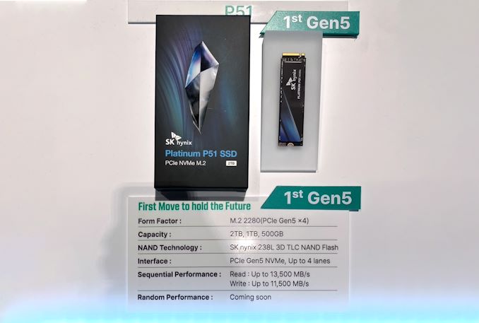
SK hynix is set to unveil their first Gen5 consumer NVMe SSD lineup shortly, based on the products at display in their GTC 2024 booth. The Platinum P51 M.2 2280 NVMe SSD will take over flagship duties from the Platinum P41 that has been serving the market for more than a year.
Similar to the Gold P31 and the Platinum P41, the Platinum P51 also uses an in-house SSD controller. The key updates are the move to PCIe Gen5 and the use of SK hynix's 238L TLC NAND. Other details are scarce, and we have reached out for additional information.
| SK hynix Platinum P51 Gen5 NVMe SSD Specifications | ||||
| Capacity | 500 GB | 1 TB | 2 TB | |
| Controller | SK hynix In-House (Alistar) | |||
| NAND Flash | SK hynix 238L 3D TLC NAND at ?? MT/s ('4D' with CMOS circuitry under the NAND as per SK hynix marketing) | |||
| Form-Factor, Interface | M.2-2280, PCIe 5.0 x4, NVMe 2.0 | |||
| Sequential Read | 13500 MB/s | |||
| Sequential Write | 11500 MB/s | |||
| Random Read IOPS | TBD | |||
| Random Write IOPS | TBD | |||
| SLC Caching | Yes | |||
| TCG Opal Encryption | TBD | |||
| Warranty | TBD | |||
| Write Endurance | TBD | TBD | TBD | |
Only the peak sequential access numbers were available at the GTC booth, indicating that the drive's firmware is still undergoing tweaks. It is also unclear how these numbers are going to vary based on capacity. Availability and pricing are also not public yet.
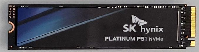
This is a significant launch for the Gen5 consumer SSD market, where the number of available options are quite limited. The Phison E26 controller and Micron's B58R NAND combination is already in its second generation (with the NAND operating at 2400 MT/s in the newest avatar), but other vertically integrated vendors such as Samsung, Western Digital / Kioxia, and SK hynix (till now) are focusing more on the Gen4 market which has much higher adoption.
We will update the piece with additional information once the specifications are officially available.
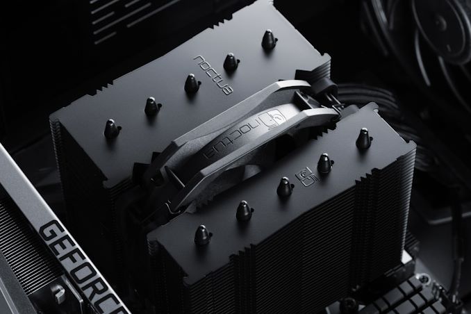
Today, Noctua announced the launch of its NH-D12L chromax.black CPU cooler, an all-black version of the existing NH-D12L. The cooler sports not only a coat of mattte black paint, but also a relatively short height of 145mm, which Noctua says makes the NH-D12L suitable for slimmer cases and 4U server racks.
Having launched in 2022, the NH-D12L is essentially a shorter version of the NH-U12A, which stands at 158mm tall. While plenty of cases have the room for a cooler that tall, not all do (especially small form factor cases). The NH-D12L exists to offer similar performance as the NH-U12A but for cases where 145mm would fit but 158mm wouldn’t. However, the NH-D12L has just a single 120mm NF-A12x25 fan, whereas the NH-U12A has two. Additionally, the NH-D12L has five heatpipes to the NH-U12A’s seven. These two factors mean the NH-D12L can’t quite catch up to the NH-U12A when it comes to cooling capacity.
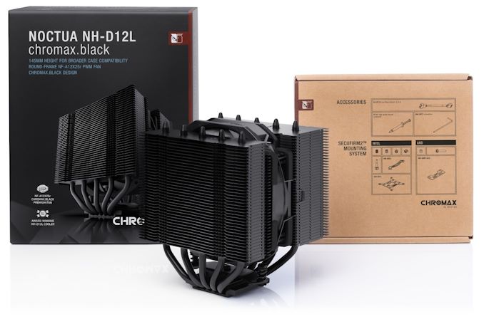
The chromax.black model is practically identical to the original, but features Noctua’s popular black motif. It should perform the same, and its SecuFirm 2 mounting hardware supports the same sockets: AMD’s AM4 and AM5, and Intel’s LGA 1700 and LGA 1851 for upcoming Arrow Lake CPUs. Despite its compact design, the NH-D12L also has “100% RAM compatibility” for sticks with tall heatspreaders, which sometimes pose clearance issues with air coolers.
The NH-D12L chromax.black also comes with the usual Noctua accessories: a screwdriver, NH-T1 thermal paste, and a four-pin low-noise adapter for the NF-A12x25 fan. Additionally, the 120mm fan is mounted to the cooler via a bracket, meaning no screws are necessary and it can be removed or installed toollessly.
At $99/€109, the NH-D12L is positioned fairly high in the market, next to larger high-end air coolers such as Corsair’s A115, as well as 240mm to 360mm AIO liquid coolers. However, the NH-D12L holds a substantial advantage in its size and compatibility, and while many of these high-end air coolers are 160mm tall or more, the NH-D12L is just 145mm. In some cases, even 15mm could make a big difference.

SK Hynix said that it had started volume production of its HBM3E memory and would supply it to a customer in late March. The South Korean company is the second DRAM producer to announce mass production of HBM3E, so the market of ultra-high-performance memory will have some competition, which is good for companies that plan to use HBM3E.
According to specifications, SK Hynix's HBM3E known good stack dies (KGSDs) feature data transfer rates up to 9.2 GT/s, a 1024-bit interface, and a bandwidth of 1.18 TB/s, which is massively higher than the 6.4 GT/s and 819 GB/s offered by HBM3. The company does not say whether it mass produces 8Hi 24GB HBM3E memory modules or 12Hi 36GB HBM3E devices, but it will likely begin its HBM3E ramp from lower-capacity products as they are easier to make.
We already know that SK Hynix's HBM3E stacks employ the company's advanced Mass Reflow Molded Underfill (MR-RUF) technology, which promises to reduce heat dissipation by 10%. This technology involves the use of an enhanced underfill between DRAM layers, which not only improves heat dissipation but also reduces the thickness of HBM stacks. As a result, 12-Hi HBM stacks can be constructed that are the same height as 8-Hi modules. However, this does not necessarily imply that the stacks currently in mass production are 12-Hi HBM3E stacks.
Although the memory maker does not officially confirm this, SK Hynix's 24GB HBM3E stacks will arrive just in time to address NVIDIA's Blackwell accelerator family for artificial intelligence and high-performance computing applications.
"With the success story of the HBM business and the strong partnership with customers that it has built for years, SK Hynix will cement its position as the total AI memory provider," said Sungsoo Ryu, Head of HBM business at SK Hynix. As a result, NVIDIA will have access to HBM3E memory from multiple suppliers with both Micron and SK Hynix.
Meanwhile, AMD recently confirmed that it was looking forward to expanding its Instinct MI300-series lineup for AI and HPC applications with higher-performance memory configurations, so SK Hynix's HBM3E memory could also be used for this.
Last year, NVIDIA introduced its cuLitho software library, which promises to speed up photomask development by up to 40 times. Today, NVIDIA announced a partnership with TSMC and Synopsys to implement its computational lithography platform for production use, and use the company's next-generation Blackwell GPUs for AI and HPC applications.
The development of photomasks is a crucial step for every chip ever made, and NVIDIA's cuLitho platform, enhanced with new generative AI algorithms, significantly speeds up this process. NVIDIA says computational lithography consumes tens of billions of hours per year on CPUs. By leveraging GPU-accelerated computational lithography, cuLitho substantially improves over traditional CPU-based methods. For example, 350 NVIDIA H100 systems can now replace 40,000 CPU systems, resulting in faster production times, lower costs, and reduced space and power requirements.
NVIDIA claims its new generative AI algorithms provide an additional 2x speedup on the already accelerated processes enabled through cuLitho. This enhancement is particularly beneficial for the optical proximity correction (OPC) process, allowing the creation of near-perfect inverse masks to account for light diffraction.
TSMC says that integrating cuLitho into its workflow has resulted in a 45x speedup of curvilinear flows and an almost 60x improvement in Manhattan-style flows. Curvilinear flows involve mask shapes represented by curves, while Manhattan mask shapes are restricted to horizontal or vertical orientations.
Synopsys, a leading developer of electronic design automation (EDA), says that its Proteus mask synthesis software running on the NVIDIA cuLitho software library has accelerated computational workloads compared to current CPU-based methods. This acceleration is crucial for enabling angstrom-level scaling and reducing turnaround time in chip manufacturing.
The collaboration between NVIDIA, TSMC, and Synopsys represents a significant advancement in semiconductor manufacturing in general and cuLitho adoption in particular. By leveraging accelerated computing and generative AI, the partners are pushing semiconductor scaling possibilities and opening new innovation opportunities in chip designs.
Already solidly in the driver’s seat of the generative AI accelerator market at this time, NVIDIA has long made it clear that the company isn’t about to slow down and check out the view. Instead, NVIDIA intends to continue iterating along its multi-generational product roadmap for GPUs and accelerators, to leverage its early advantage and stay ahead of its ever-growing coterie of competitors in the accelerator market. So while NVIDIA’s ridiculously popular H100/H200/GH200 series of accelerators are already the hottest ticket in Silicon Valley, it’s already time to talk about the next generation accelerator architecture to feed NVIDIA’s AI ambitions: Blackwell.
We're here in sunny San Jose California for the return of an event that's been a long-time coming: NVIDIA's in-person GTC. The Spring 2024 event, NVIDIA's marquee event for the year, promises to be a big one for NVIDIA, as the company is due to deliver updates on its all-important datacenter accelerator products – the successor to the GH100 GPU and its Hopper architecture – along with NVIDIA's other professional/enterprise hardware, networking gear, and, of course, a slew of software stack updates.
In the 5 years since NVIDIA was last able to hold a Spring GTC in person, a great deal has changed for the company. They're now the third biggest company in the world, thanks to explosive sales growth (and even further growth expectations) due in large part to the combination of GPT-3/4 and other transformer models, and NVIDIA's transformer-optimized H100 accelerator. As a result, NVIDIA is riding high in Silicon Valley, but to keep doing so they also will need to deliver the next big thing to push the envelope on performance, and keep a number of hungry competitors off their turf.
Headlining today's keynote is, of course, NVIDIA CEO Jensen Huang, whose kick-off address has finally outgrown the San Jose Convention Center. As a result, Huang is filling up the local SAP Center arena instead. Suffice it to say, it's a bigger venue for a bigger audience for a [i]much[/i] bigger company.
So come join the AnandTech crew for our live blog coverage of NVIDIA's biggest enterprise keynote in years. The presentation kicks off at 1pm Pacific, 4pm Eastern, 20:00 UTC.
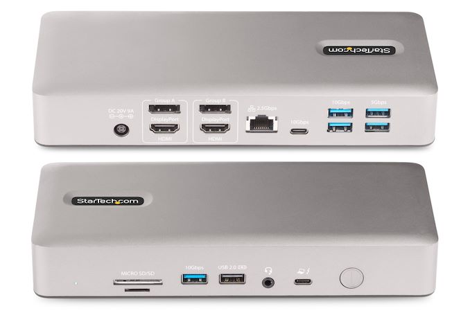
StarTech.com has introduced its latest Thunderbolt 4/USB4 docking station, which has a plethora of ports and supports four display outputs. This makes it suitable for 4Kp60 quad-monitor setups often used for professional applications. The Thunderbolt 4 Quad Display Docking Station can also deliver up to 98W of power to the host, which is enough to feed a high-end laptop, such as Apple's MacBook Pro 16.
StarTech's 15-in-1 docking (132N-TB4USB4DOCK) has pretty much everything that one comes to expect from a dock engineered explicitly for demanding professionals, such as those involved in photography, content creation, video production, and computer-aided design. The unit comes with one Thunderbolt 4/USB 4 port with a 98W power delivery capability to connect to the host, a 2.5 GbE adapter, six USB Type-A ports (three supporting 10 Gbps, two supporting 5 Gbps, and one being USB 2.0 for up to 7.5W charging), one USB Type-C connector (at 10 Gbps), four display outputs (two DP 1.4, two HDMI 2.1), an SD Card reader with UHS-II, a microSD card reader with UHS-II, and a 3.5-mm audio jack.
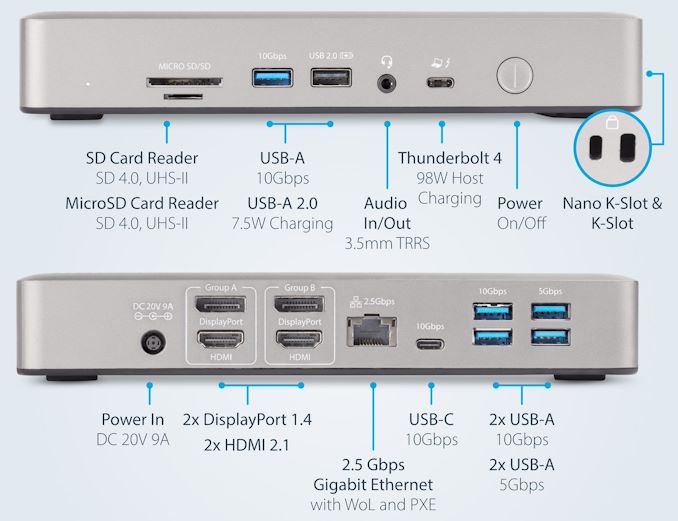
The dock's main selling feature is, its support for up to four displays. Of course, this is a valuable capability, but it has a couple of catches. The device can support four 4Kp60 displays when connected to a laptop featuring Intel's 12th or 14th Generation Core processor using a Thunderbolt 4 or USB 4 connector and with DSC enabled. With AMD Ryzen 6000 and Intel's 11th Gen Core-based systems, only three 4Kp60 displays are supported. Meanwhile, with MacBooks, users must get on with two 5Kp60 or one 6Kp60 display. The good news is that the Thunderbolt 4 Quad Display Docking Station requires no drivers and works seamlessly with MacOS, Windows, and ChromeOS.
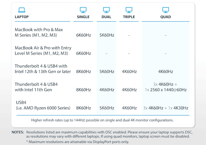
The docking station has a 180W power supply, so it can simultaneously charge a laptop and power on all the remaining ports.
Thunderbolt 4 and USB 4 docks with rich capabilities are not cheap as they have to pack loads of quite expensive controllers, and StarTech's 15-in-1 docking station is no exception, as it costs $330.99.
The StarTech.com Thunderbolt 4 Quad Display Docking Station is available for purchase directly from the company and through various IT resellers and distributors such as CDW, Amazon, Ingram Micro, TD SYNNEX, and D&H.
With the launch of their flagship Snapdragon 8 SoC firmly behind them now, Qualcomm this morning is turning their collective head towards the premium market with the launch of another new Snapdragon 8 family SoC, the Snapdragon 8s Gen 3. The first of Qualcomm’s ‘s’-subseries of down-market parts to be released under the Snapdragon 8 banner, the Snapdragon 8s Gen 3 (8sG3) is intended to be a bridge part between the last-gen flagship 8 Gen 2 and current-gen flagship 8 Gen 3, offering a not-quite-flagship experience at a lower price point than Qualcomm’s top SoC. The new SoC is set to be available globally, with the first phones announced this month, though as is often the case for Qualcomm’s “premium” market SoCs, it looks like only Chinese handset OEMs will be picking up the chip, at least initially.
Although Qualcomm prefers to draw comparisons to their current gen flagship Snapdragon 8 Gen 3, the Snapdragon 8s Gen 3 is by and large and enhanced version of the Snapdragon 8 Gen 2. Many of the hardware blocks of the 8G2 have been carried over to the new chip – either in whole or in terms of functionality – a process that is made very easy thanks to the fact that Qualcomm is building the chip on the same TSMC 4nm node as the 8G2 and 8G3. Compared to the 8G2 then, there are two key differentiators for the 8sG3: a newer CPU complex lifted from the 8G3, and official on-device generative AI support.
| Qualcomm Snapdragon 8 SoCs | ||||
| SoC | Snapdragon 8 Gen 3 (SM8650) |
Snapdragon 8s Gen 3 (SM8635) |
Snapdragon 8 Gen 2 (SM8550) |
|
| CPU | 1x Cortex-X4 @ 3.3GHz 3x Cortex-A720 @ 3.2GHz 2x Cortex-A720 @ 3.0GHz 2x Cortex-A520 @ 2.3GHz 12MB sL3 |
1x Cortex-X4 @ 3.0GHz 4x Cortex-A720 @ 2.8GHz 3x Cortex-A520 @ 2.0GHz |
1x Cortex-X3 @ 3.2GHz 2x Cortex-A715 @ 2.8GHz 2x Cortex-A710 @ 2.8GHz 4x Cortex-A510 @ 2.0GHz 8MB sL3 |
|
| GPU | Adreno (Hardware RT & Global Illum.) |
Adreno (Hardware RT) |
Adreno (Hardware RT) |
|
| DSP / NPU | Hexagon | Hexagon | Hexagon | |
| Memory Controller |
4x 16-bit CH @ 4800MHz LPDDR5X / 76.8GB/s |
4x 16-bit CH @ 4200MHz LPDDR5X / 67.2GB/s |
4x 16-bit CH @ 4200MHz LPDDR5X / 67.2GB/s |
|
| ISP/Camera | Triple 18-bit Spectra ISP 1x 200MP or 108MP with ZSL or 64+36MP with ZSL or 3x 36MP with ZSL 8K HDR video & 64MP burst capture |
Triple 18-bit Spectra ISP 1x 200MP or 108MP with ZSL or 64+36MP with ZSL or 3x 36MP with ZSL 4K HDR video & 64MP burst capture |
Triple 18-bit Spectra ISP 1x 200MP or 108MP with ZSL or 64+36MP with ZSL or 3x 36MP with ZSL 8K HDR video & 64MP burst capture |
|
| Encode/ Decode |
8K30 / 4K120 10-bit H.265 H.265, VP9, AV1 Decoding Dolby Vision, HDR10+, HDR10, HLG 720p960 SlowMo |
4K60 10-bit H.265 H.265, VP9, AV1 Decoding Dolby Vision, HDR10+, HDR10, HLG 1080p240 SlowMo |
8K30 / 4K120 10-bit H.265 H.265, VP9, AV1 Decoding Dolby Vision, HDR10+, HDR10, HLG 720p960 SlowMo |
|
| Integrated Radio |
FastConnect 7800 Wi-FI 7 + BT 5.4 2x2 MIMO |
FastConnect 7800 Wi-FI 7 + BT 5.4 2x2 MIMO |
FastConnect 7800 Wi-FI 7 + BT 5.3 2x2 MIMO |
|
| Integrated Modem | X75 integrated 3GPP Rel 18 (5G NR Sub-6 + mmWave) DL = 10000 Mbps UL = 3500 Mbps |
X70 integrated 3GPP Rel 17 (5G NR Sub-6 + mmWave) DL = 5000 Mbps UL = 3500 Mbps |
X70 integrated 3GPP Rel 17 (5G NR Sub-6 + mmWave) DL = 10000 Mbps UL = 3500 Mbps |
|
| Mfc. Process | TSMC 4nm | TSMC 4nm | TSMC 4nm | |
Starting with the CPU complex, Qualcomm is implementing Arm’s latest generation of Armv9 CPU cores here, meaning a mix of the Cortex-X4, Cortex-A720, and Cortex-A520. Relative to the flagship 8G3, the 8sG3 gives up one of its performance cores for another efficiency core, shifting the design from a 1/5/2 configuration to a 1/4/3 configuration – the same as the 8G2. The 8sG3 also loses some frequency headroom in the process, with the X4 prime core dropping from 3.3GHz to 3.0GHz, and the other CPU cores following similarly along.
Still, the 8sG3 should outperform the 8G2 in CPU tasks, which is the primary reason for replacing the CPU complex at all. Qualcomm is basically looking to offer an 8G2 with better CPU performance and energy efficiency, and using Arm’s latest CPU cores will be how they deliver on that.
Outside of the CPU complex, however, most of the rest of the functional blocks are either lifted from the 8G2, or are the same generation teams of features. This means the 8sG3’s integrated GPU offers hardware raytracing, for example, but not the global illumination support that was introduced for the flagship 8G3. The memory controller is also otherwise identical to the 8G2, with the SoC supporting a maximum of 24GB of LPDDDRX-8400.
The video recording and decoding capabilities of the 8sG3 are a distinct downgrade from the other Snapdragon 8 SoCs, however. Qualcomm has retained their trio of 18-bit Spectra ISPs – so the SoC can support up to 3 cameras – but all 8K support has been excised entirely. Instead, the 8sG3 can only record video at up to 4K, and even then only at 60fps, half the framerate of the 8G3/8G2. Slow-mo video capture has also been altered, as well; Qualcomm lists 1080p240 for this mode rather than 720p960. The higher resolution will no doubt be appreciated, but less so if this means it’s not possible to record above 240fps.
The lack of 8K video support also applies to the SoC’s video decode block, which can only decode videos up to 4K in resolution. Qualcomm has otherwise kept all of the underlying features of the video decode block at parity, however, so the 8sG3 gets support for AV1 decoding, along with Dolby Vision HDR.
Meanwhile, the DSP/NPU situation on the 8sG3 is a mixed bag. Officially, this SoC supports generative AI models (up to 10B parameters in size), something the 8G2 and its NPU were not capable of, and is otherwise only available on the 8G3. However, according to Qualcomm this is not the same generation of NPU IP as on the 8G3, and among other things it lacks support for speculative decoding (and I don’t see any mention of the newer NPU’s micro-tile inferencing improvements). So by all appearances, this is just the 8G2 NPU. Still, Qualcomm has at least rolled out some software/firmware updates to improve its functionality, giving it additional AI functionality right as exuberance for that is through the roof.
Finally, the comms side of the 8sG3 is essentially a slower version of the 8G2. Qualcomm is once again using their Snapdragon X70 integrated modem here, a 5G Release 17-generation design that offers 2x2 MIMO on mmWave, and 4x4 MIMO on sub-6G. Max upload speeds are unchanged, at 3.5Gbps, however max download speeds for the 8sG3 are 5Gbps, half that of the 8G2 (and 8G3). Paired with the X70 modem is Qualcomm’s FastConnect 7800 system, which offers Wi-Fi 7 support with 2x2 MIMO, as well as Bluetooth 5.4. The dual BT antenna feature from the other Snapdragon 8 chips has also made it over for this part.
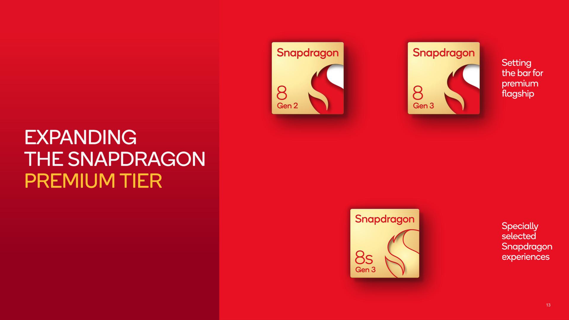
Overall, the Snapdragon 8s Gen 3 is intended to occupy a very specific niche within Qualcomm’s SoC lineup, offering a cheaper alternative to their flagship SoC without giving up too many features. The marketing messaging behind the chip is made somewhat complicated by the fact that last year at this time Qualcomm launched the Snapdragon 7+ Gen 2 for the premium market, which at least partially overlaps what they’re trying to do with the 8sG3. None the less, Qualcomm insists there’s a market for chips between the Snapdragon 7 series and the flagship Snapdragon 8 SoC, and so here we are.
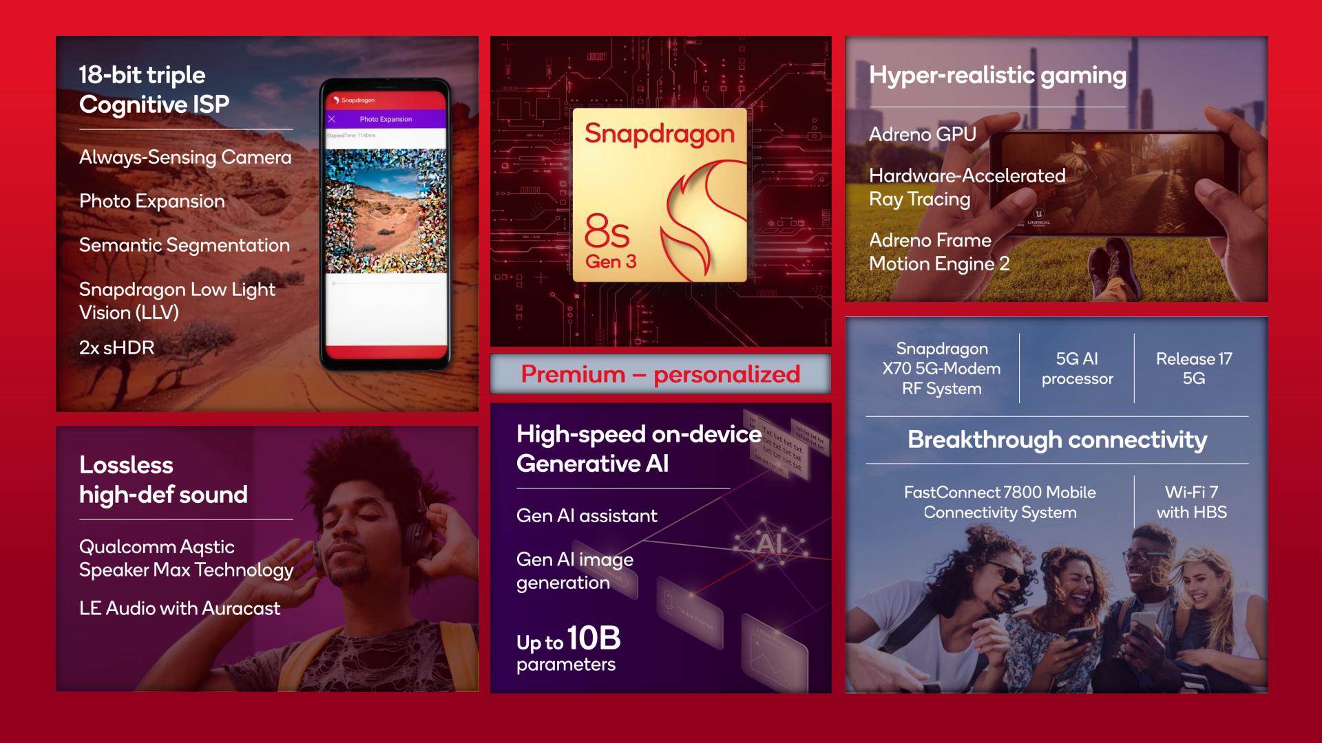
Absent another 7+ chip this year, it’s hard to see the 8sG3 as anything other than the 7+’s successor. Still, where the 7+ was a souped-up 7, the 8sG3 is clearly a down-market 8, so it has some significant hardware advantages, particularly when it comes to memory bandwidth. It may just be that Qualcomm aimed a bit too low for the premium market with the specs for the 7+, so this is an attempt to aim a bit higher.
In any case, expect to see the Snapdragon 8s Gen 3 picked up by many of the usual Chinese handset OEMs, including Honor, iQOO, realme, Redmi and Xiaomi. The first phones are expected to be announced this month.


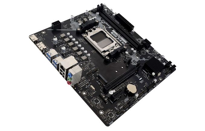
BIOSTAR has launched its AM5-based A620MS motherboard today, bringing a new low-end option for PC users on a budget. Though BIOSTAR has not disclosed what MSRP it the A620MS motherboard will carry, the specifications of the board make it clear that it targets the lowest-end segment of the market, though it makes use of the regular A620 chipset instead of the even less expensive A620A chipset.
The A620MS sports some features typical for mATX A620 boards (which make up the vast majority of current models): two DDR5 DIMM slots that support up to two 48GB sticks, an M.2 PCIe 4.0 slot for SSDs, four SATA III ports, and a PCIe Gen4 x16 slot. The motherboard also has four debug LEDs for diagnosing CPU, RAM, GPU, and booting errors.
Meanwhile the rear I/O features a one gigabit Ethernet port, four USB 3.2 ports, analog audio jacks, two USB 2.0 ports, an HDMI 1.4 port, and DisplayPort 1.2. Though there are some more fully-featured A620 motherboards available with more ports operating at a higher specification, but the rear I/O is more or less par for the course when it comes to A620.
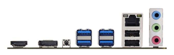
However, there are other things about BIOSTAR’s A620MS that implies it will be quite low-end for an A620 motherboard. It has just eight total voltage regulator modules (VRMs), which appear to be in a 6+2 or 6+1+1 phase configuration. This isn’t as low-end as BIOSTAR could have gone (ASRock offers a 4+1+1 stage board), but it is still very sparing in VRM stages compared to most other A620 motherboards. These VRMs are also not covered by a heatsink, which is also typical for boards in this segment, as they're normally paired with equally chip 65W(ish) chips.
BIOSTAR doesn’t list any official CPU restrictions in either its press release or its specification sheet; instead, the company simply lists the motherboard as compatible with Ryzen 7000 and future Ryzen 8000 processors.
While the market for AM5 motherboards includes plenty of B650(E) and X670(E) models, there’s only a handful of A620 boards in total. On Newegg, there are 14 different motherboards available, and many only differ slightly in respect to things like form factor. The cheapest of these cost $75 to $100, and while BIOSTAR didn’t reveal what price we should expect of its A620MS board, given its specifications, we expect it will land in that same $75 to $100 region.

The DNA Data Storage Alliance introduced its inaugural specifications for DNA-based data storage this week. This specification outlines a method for encoding essential information within a DNA data archive, crucial for developing and commercializing an interoperable storage ecosystem.
DNA data storage uses short strings of deoxyribonucleic acid (DNA) called oligonucleotides (oligos) mixed together without a specific physical ordering scheme. This storage media lacks a dedicated controller and an organizational means to understand the proximity of one media subcomponent to another. DNA storage differs significantly from traditional media like tape, HDD, and SSD, which have fixed structures and controllers that can read and write data from the structured media. DNA's lack of physical structure requires a unique approach to initiate data retrieval, which brings its peculiarities regarding standardization.
To address this, the SNIA DNA Archive Rosetta Stone (DARS) working group, part of the DNA Data Storage Alliance, has developed two specifications, Sector Zero and Sector One, to facilitate the process of starting a DNA archive.
Sector Zero serves as the starting point, providing minimal details necessary for the archive reader to identify the entity responsible for synthesizing the DNA (e.g., Dell, Microsoft, Twist Bioscience) and the CODEC used for encoding Sector One (e.g., Super Codec, Hyper Codec, Jimbob's Codec). Sector Zero consists of 70 bases: the first 35 bases identify the vendor, and the second 35 bases identify the codec. The information in Sector Zero enables access and decoding of data stored in Sector One. The amount of data stored in SZ is small and fits into a single oligonucleotide.
Sector One expands on this by including a description of the contents, a file table, and parameters required for transferring data to a sequencer. This specification ensures that the main body of the archive is accessible and readable, paving the way for data retrieval. Sector One contains exactly 150 bases and will span multiple oligonucleotides.
"A key goal of the DNA Data Storage Alliance is to set and publish specifications and standards that allow an interoperable DNA data storage ecosystem to grow," said Dave Landsman, of the DNA Data Storage Alliance Board of Directors. "With the publishing of the Alliance's first specifications, we take an important step in achieving that goal. Sector Zero and Sector One are now publicly available, allowing companies working in the space to adopt and implement."
The DNA Data Storage Alliance is led by Catalog Technologies, Inc., Quantum Corporation, Twist Bioscience Corporation, and Western Digital (though we are unsure whether Western Digital's NAND or HDD division is responsible for developing the specification). Meanwhile, numerous industry giants, including Microsoft, support the DNA Data Storage Alliance.
Source: SNIA